- Forums
- Product Forums
- General Purpose MicrocontrollersGeneral Purpose Microcontrollers
- i.MX Forumsi.MX Forums
- QorIQ Processing PlatformsQorIQ Processing Platforms
- Identification and SecurityIdentification and Security
- Power ManagementPower Management
- Wireless ConnectivityWireless Connectivity
- RFID / NFCRFID / NFC
- Advanced AnalogAdvanced Analog
- MCX Microcontrollers
- S32G
- S32K
- S32V
- MPC5xxx
- Other NXP Products
- S12 / MagniV Microcontrollers
- Powertrain and Electrification Analog Drivers
- Sensors
- Vybrid Processors
- Digital Signal Controllers
- 8-bit Microcontrollers
- ColdFire/68K Microcontrollers and Processors
- PowerQUICC Processors
- OSBDM and TBDML
- S32M
- S32Z/E
-
- Solution Forums
- Software Forums
- MCUXpresso Software and ToolsMCUXpresso Software and Tools
- CodeWarriorCodeWarrior
- MQX Software SolutionsMQX Software Solutions
- Model-Based Design Toolbox (MBDT)Model-Based Design Toolbox (MBDT)
- FreeMASTER
- eIQ Machine Learning Software
- Embedded Software and Tools Clinic
- S32 SDK
- S32 Design Studio
- GUI Guider
- Zephyr Project
- Voice Technology
- Application Software Packs
- Secure Provisioning SDK (SPSDK)
- Processor Expert Software
- Generative AI & LLMs
-
- Topics
- Mobile Robotics - Drones and RoversMobile Robotics - Drones and Rovers
- NXP Training ContentNXP Training Content
- University ProgramsUniversity Programs
- Rapid IoT
- NXP Designs
- SafeAssure-Community
- OSS Security & Maintenance
- Using Our Community
-
- Cloud Lab Forums
-
- Knowledge Bases
- ARM Microcontrollers
- i.MX Processors
- Identification and Security
- Model-Based Design Toolbox (MBDT)
- QorIQ Processing Platforms
- S32 Automotive Processing Platform
- Wireless Connectivity
- CodeWarrior
- MCUXpresso Suite of Software and Tools
- MQX Software Solutions
- RFID / NFC
- Advanced Analog
-
- NXP Tech Blogs
Programming for FS32K144HFT0MLHT
Hi Sir,
Good day.
This is IC programmer manufacturer.
Recently we support this MPN(FS32K144HFT0MLHT) with SWD and IAP(boot code).
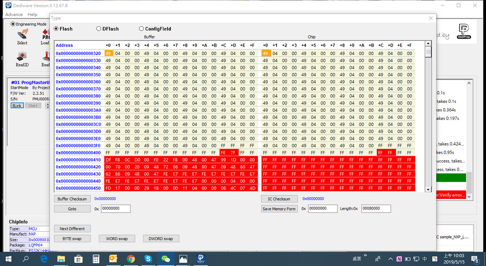
We face a issue that the content 0x7F is written at address 0x40D, and then programmer read the contents are blank(0xFF) at address 0x400 to 0x7FFFF after power cycle. if we change the content from 0x7F to 0xFF, and the content are correct at whole flash after power cycle. i think whether we have to set up the register in the initialize process and avoid the issue is happened.
Left side is content in software buffer ; Right side is content of chip.
Thank you.
Hi jackhsu, jun.chen@dediprog.com
As you can see in AN12130, Section 3.2 Erasing flash, during the Mass Erase operations, the flash configuration field is programmed to 0xFE (unsecure). Then, you cannot write the same phrase again without erasing it first.
But you can use all the FTFC commands, including Erase Sector, via SWD by accessing the FTFC registers.
Regards,
Daniel
Hi Daniel,
I am a colleague of Jack, we are responsible for this case together.
In Step 3, we execute SWD mass erase. When the operation is done 0x40F is 0xFE, others register is 0xFF.
Guess this is the reason why 0x408 - 0x40F can't be programmed.
But currently, we could not execute Erase Sector Command via SWD.
Are we only able to execute Erase Sector Command with boot code in MCU?
Hi Daniel,
Sorry for late reply.
Sorry for making confuse.
if programmer write the 0x7F/0x7D at address 0x40D (flash), the programmer reads the all 0xFF at address 0x400 ~ flash end address after power cycle. if programmer write the 0xFF at address 0x40D (flash), the programmer can read correct content from whole flash.
We use IAP method with SWD during programming, and these is the programming procedure.
Step 1. Power on
Step 2. Read SWD ID
Step 3. Execute erase command via SWD
Step 4. Load IAP code to RAM and booted.
Step 5. Send the data to IAP to write it to chip.
Step 6. Read data from chip to do verify via SWD.
Step 7. Power off
Our engineer even tried to use SWD with no IAP, and the situation is same.
We made the IAP code is refer to IAR sample code.
There is my questions.
1. Do we need to set up the register in the initialize procedure or program procedure?
2. Do we need to set up the register in the IAP code?
3. Or could you help to provide the IAP code and how to communicate it for programming.
Thank you.
Hi Jack,
First, could you please be more specific about Step 3?
What command you are using to erase the MCU?
Once the MCU is erased, is the phrase at 0x408 - 0x40F really erased?
I think that the only explanation is that the phrase is not erased.
Thank you,
BR, Daniel
Hi Jack,
Was the 0x400-0x40F phrase erased before the programming?
Why do you program the 0x40D byte to 0x7F?
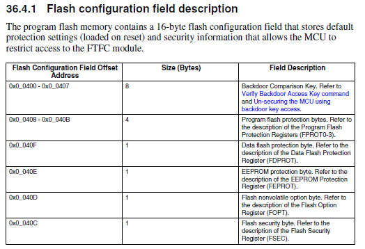
This is the FOPT byte that is loaded to the Flash Option Register (FOPT) register at reset and the 4-7 bits are reserved.
BR, Daniel
Hi Daniel,
Thanks for your reply.
Was the 0x400-0x40F phrase erased before the programming? => Yes, it is eased before the programming.
Why do you program the 0x40D byte to 0x7F? => it is customer's file, we don't know why they need to write 0x7F.
We ever used JLink to program this file as below, and it work well, and we have no idea why the issue is happened on my programming platform.
Need your help to support this case. Thank you.
https://eip.dediprog.com/ftp/download.php?path=dediprog/FS32K.hex
Hi Jack,
You wrote: "... and then programmer reads the contents are blank(0xFF) at address 0x400 to 0x7FFFF after power cycle". If the 0x40C address was 0xFF, the MCU would end up secured and the access to the flash would not be possible without another mass-ease operation. Please see the description of FSEC (36.4.4.1.4 Flash Security Register (FSEC), in the RM. rev10).
I don't have any problem loading the .hex file either using OpenSDA.
What are the programming steps that you are doing?
How do you ease the MCU?
Please refer to AN12130 Production Flash Programming Best Practices for S32K1xx MCUs
Thanks,
BR, Daniel


