- Forums
- Product Forums
- General Purpose MicrocontrollersGeneral Purpose Microcontrollers
- i.MX Forumsi.MX Forums
- QorIQ Processing PlatformsQorIQ Processing Platforms
- Identification and SecurityIdentification and Security
- Power ManagementPower Management
- MCX Microcontrollers
- S32G
- S32K
- S32V
- MPC5xxx
- Other NXP Products
- Wireless Connectivity
- S12 / MagniV Microcontrollers
- Powertrain and Electrification Analog Drivers
- Sensors
- Vybrid Processors
- Digital Signal Controllers
- 8-bit Microcontrollers
- ColdFire/68K Microcontrollers and Processors
- PowerQUICC Processors
- OSBDM and TBDML
- S32M
-
- Solution Forums
- Software Forums
- MCUXpresso Software and ToolsMCUXpresso Software and Tools
- CodeWarriorCodeWarrior
- MQX Software SolutionsMQX Software Solutions
- Model-Based Design Toolbox (MBDT)Model-Based Design Toolbox (MBDT)
- FreeMASTER
- eIQ Machine Learning Software
- Embedded Software and Tools Clinic
- S32 SDK
- S32 Design Studio
- GUI Guider
- Zephyr Project
- Voice Technology
- Application Software Packs
- Secure Provisioning SDK (SPSDK)
- Processor Expert Software
- MCUXpresso Training Hub
-
- Topics
- Mobile Robotics - Drones and RoversMobile Robotics - Drones and Rovers
- NXP Training ContentNXP Training Content
- University ProgramsUniversity Programs
- Rapid IoT
- NXP Designs
- SafeAssure-Community
- OSS Security & Maintenance
- Using Our Community
-
- Cloud Lab Forums
-
- Knowledge Bases
- ARM Microcontrollers
- i.MX Processors
- Identification and Security
- Model-Based Design Toolbox (MBDT)
- QorIQ Processing Platforms
- S32 Automotive Processing Platform
- Wireless Connectivity
- CodeWarrior
- MCUXpresso Suite of Software and Tools
- MQX Software Solutions
-
- RSS フィードを購読する
- トピックを新着としてマーク
- トピックを既読としてマーク
- このトピックを現在のユーザーにフロートします
- ブックマーク
- 購読
- ミュート
- 印刷用ページ
Problem with UJA1169
- 新着としてマーク
- ブックマーク
- 購読
- ミュート
- RSS フィードを購読する
- ハイライト
- 印刷
- 不適切なコンテンツを報告
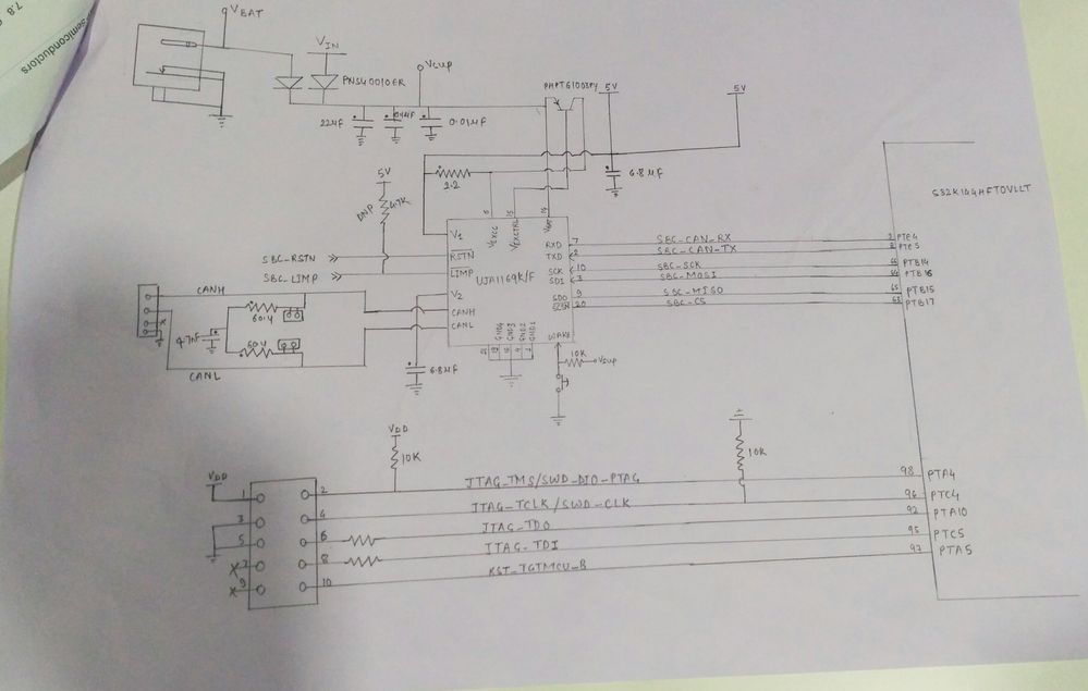
This is UJA1169TK/F connected to S32K.S32K is supplied power by USB. I have connected 120 ohms termination resistor between CANH and CANL. The positive terminal of the battery is connected to VBAT and negative is connected to ground. Since both UJA1169 and S32K are working at 5V, all signal pins are directly connected to corresponding S32K pins. Still, I am not getting any signal. Please help me out. What is wrong with this circuit?
- 新着としてマーク
- ブックマーク
- 購読
- ミュート
- RSS フィードを購読する
- ハイライト
- 印刷
- 不適切なコンテンツを報告
1. I don't think it has anything to do with wakeup pin.
2. UJA1169 only a slave device, clock provide by MCU. Since 1169 didn't work properly, I think I should still check 1169
3. how about RST pin with UJA1169? Is RST pin high?
- 新着としてマーク
- ブックマーク
- 購読
- ミュート
- RSS フィードを購読する
- ハイライト
- 印刷
- 不適切なコンテンツを報告
This is the circuit, I had uploaded earlier which you were not to able see. Now, we are getting output at pin V1 but it falls from 5V to 0V slowly. The output is constant at 5V. How to clamp V1 at 5V? What could be done to solve this?
- 新着としてマーク
- ブックマーク
- 購読
- ミュート
- RSS フィードを購読する
- ハイライト
- 印刷
- 不適切なコンテンツを報告
I got your first two points.
I have kept Reset at active low.
Do you think Limp pin has anything to do with my UJA1169 ? I have given LIMP a 10k pull up resistor connected to 5V.
- 新着としてマーク
- ブックマーク
- 購読
- ミュート
- RSS フィードを購読する
- ハイライト
- 印刷
- 不適切なコンテンツを報告
you can see about LIMP pin at datasheet. If you don't need this indication, you can keep it floating.
LIMP output
The dedicated LIMP pin can be used to enable so called ‘limp home’ hardware in the event of a serious ECU failure. Detectable failure conditions include SBC overtemperature events, loss of watchdog service, short-circuits on pins RSTN or V1 and user-initiated or external reset events (see Figure 7). The LIMP pin is a battery-robust, active-LOW, open-drain output. The LIMP pin can also be forced LOW by setting bit LHC in the Fail-safe control register (Table 14).
- 新着としてマーク
- ブックマーク
- 購読
- ミュート
- RSS フィードを購読する
- ハイライト
- 印刷
- 不適切なコンテンツを報告
I think there is no problem from the hardware circuit.
I think you should check from the following points:
1. Make sure the UJA1169 is working. if it's a new UJA1169 chip and never been configured, V1 and V2 should be 5V。
2. make sure the MCU in working.
3. Make sure the command you sent is correct。 e.g. : you can read 7E register to get chip information and the command is FD. check if the SBC return to you ...
- 新着としてマーク
- ブックマーク
- 購読
- ミュート
- RSS フィードを購読する
- ハイライト
- 印刷
- 不適切なコンテンツを報告
I am getting 5V at V2 but not getting output at V1. Can you tell me the possible reasons? What should I do?
- 新着としてマーク
- ブックマーク
- 購読
- ミュート
- RSS フィードを購読する
- ハイライト
- 印刷
- 不適切なコンテンツを報告
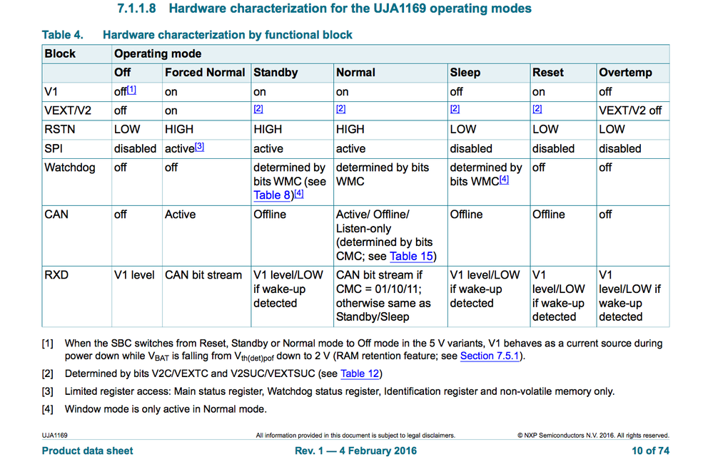
can you confirm UJA1169 at which mode?
- 新着としてマーク
- ブックマーク
- 購読
- ミュート
- RSS フィードを購読する
- ハイライト
- 印刷
- 不適切なコンテンツを報告
Hello Cui,
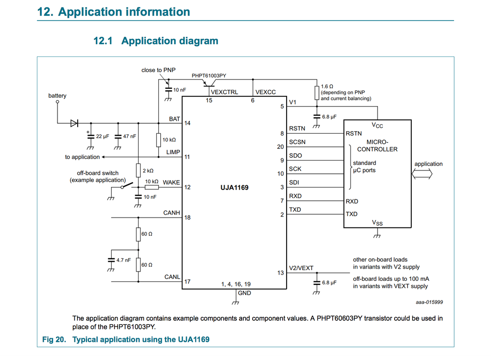
Just to fill you in. Me and Shreya are part of a same team working for an automotive company. We are using S32k Micro-controller (S32K144EVB) as part of our embedded system. Now we are making our own custom PCB using FS32K144HFT0VLLT MCU and UJA1169. Now my micro-controller can be successfully programmed, although when i make connections of this MCU to my UJA1169 as shown in the datasheet (page 64), somehow i am not able to receive data on my computer. Like Shreya said, V1 doesn't show any output and V2 gives me 6Volts. I have tried this with plenty of UJA1169 IC's and getting the same result. So, i am sure my IC is soldered just fine on the breakout board. What possible reasons could you suggest me ? I'd really appreciate your expertise.
Thank you..
- 新着としてマーク
- ブックマーク
- 購読
- ミュート
- RSS フィードを購読する
- ハイライト
- 印刷
- 不適切なコンテンツを報告
Hello,
can you show me the schematic about UJA1169? Do you used an external PNP?
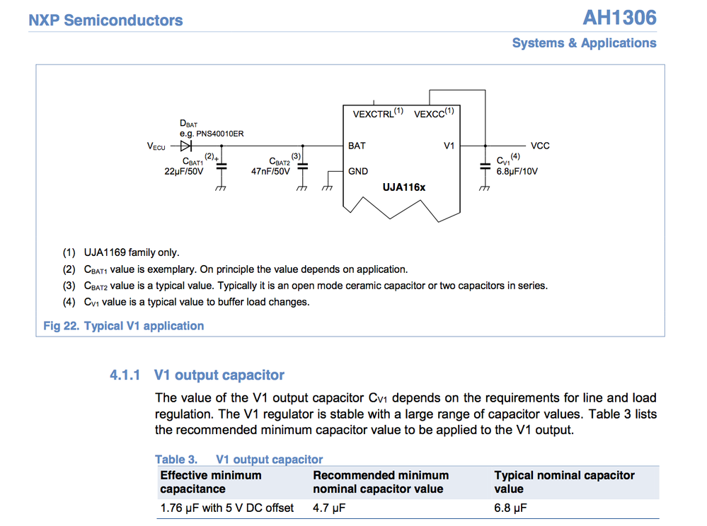
If you don't use an external pnp,I think you should connect Vexcc pin and V1 pin. and connect a capacitor to ground.
please see picture from AN1306.
I think the hardware design should be checked before the V1 is correctly output.
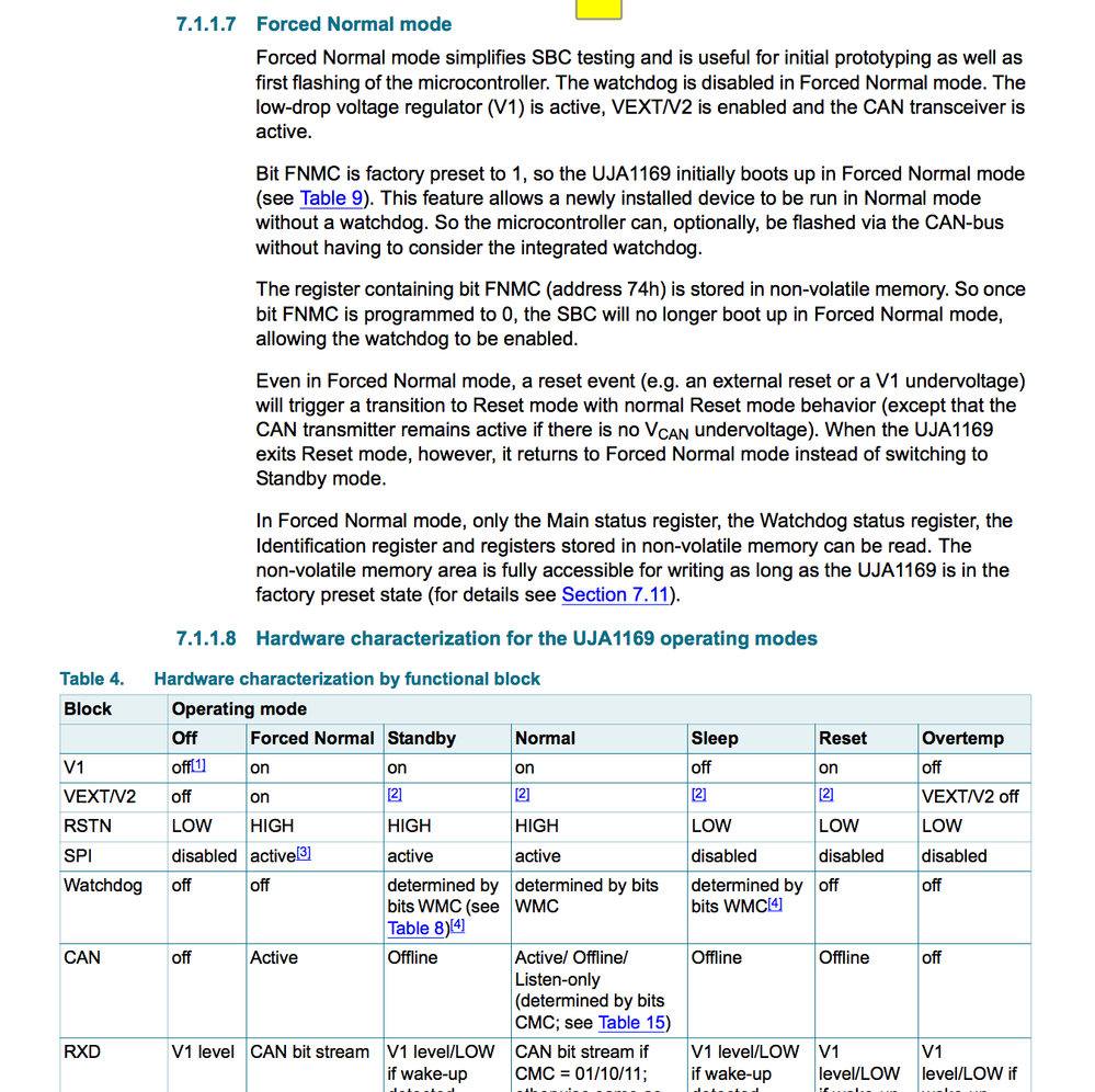
In general, if it is a new chip, V1 should have a 5V output after power-on.bacause it should at "forced normal mode" you can find it at datasheet page10.
PS: @SHREYA SINGH I am very sorry that I can't open Google here.so I can't see what your share.
- 新着としてマーク
- ブックマーク
- 購読
- ミュート
- RSS フィードを購読する
- ハイライト
- 印刷
- 不適切なコンテンツを報告
Thank you for your response. I am not using PNP transistor in my schematic and the rest of the application diagram is same as shown on the page 64 of datasheet.
I have tried connecting PNP as well but haven't got any result therefore i am not connecting it now. Should it be important to connect the PNP ?
Yes, it is a new chip and i am still not getting any output at V1. Can you tell me if the following could be the possible reasons ?
1. It has something to do with the wake-up pin (pin no 12) ?
2. My UJA1169 chip is out of sync with my FS32K144HFT0VLLT micro-controller due to any clock issue in my firmware?
- 新着としてマーク
- ブックマーク
- 購読
- ミュート
- RSS フィードを購読する
- ハイライト
- 印刷
- 不適切なコンテンツを報告
Ok, I will do that.I am attaching the complete circuit. Is everything correct?
