- Forums
- Product Forums
- General Purpose MicrocontrollersGeneral Purpose Microcontrollers
- i.MX Forumsi.MX Forums
- QorIQ Processing PlatformsQorIQ Processing Platforms
- Identification and SecurityIdentification and Security
- Power ManagementPower Management
- Wireless ConnectivityWireless Connectivity
- RFID / NFCRFID / NFC
- MCX Microcontrollers
- S32G
- S32K
- S32V
- MPC5xxx
- Other NXP Products
- S12 / MagniV Microcontrollers
- Powertrain and Electrification Analog Drivers
- Sensors
- Vybrid Processors
- Digital Signal Controllers
- 8-bit Microcontrollers
- ColdFire/68K Microcontrollers and Processors
- PowerQUICC Processors
- OSBDM and TBDML
- S32M
-
- Solution Forums
- Software Forums
- MCUXpresso Software and ToolsMCUXpresso Software and Tools
- CodeWarriorCodeWarrior
- MQX Software SolutionsMQX Software Solutions
- Model-Based Design Toolbox (MBDT)Model-Based Design Toolbox (MBDT)
- FreeMASTER
- eIQ Machine Learning Software
- Embedded Software and Tools Clinic
- S32 SDK
- S32 Design Studio
- GUI Guider
- Zephyr Project
- Voice Technology
- Application Software Packs
- Secure Provisioning SDK (SPSDK)
- Processor Expert Software
-
- Topics
- Mobile Robotics - Drones and RoversMobile Robotics - Drones and Rovers
- NXP Training ContentNXP Training Content
- University ProgramsUniversity Programs
- Rapid IoT
- NXP Designs
- SafeAssure-Community
- OSS Security & Maintenance
- Using Our Community
-
- Cloud Lab Forums
-
- Knowledge Bases
- ARM Microcontrollers
- i.MX Processors
- Identification and Security
- Model-Based Design Toolbox (MBDT)
- QorIQ Processing Platforms
- S32 Automotive Processing Platform
- Wireless Connectivity
- CodeWarrior
- MCUXpresso Suite of Software and Tools
- MQX Software Solutions
-
- Home
- :
- 产品论坛
- :
- S12 / MagniV微控制器
- :
- Re: GDU Charge Pump "CP Pin" Can Not Output The Correct Wave(Frequence and Duty) I Want
GDU Charge Pump "CP Pin" Can Not Output The Correct Wave(Frequence and Duty) I Want
GDU init as follwing:
void initGDU(void)
{
GDUE_GCPE = 1; // charge pump
GDUE_GCSE0 = 1; // enable Current Sense Amplifier 0
GDUF = 0xff; // Flag Register - clear all error flags
GDUBCL = 0x0F; // Set coil current limit to maximum 750mA
GDUCLK1_GBOCD = 0b10001; // Set boost frequency ~ 0.52MHz
GDUCLK1_GBODC = 0b11; // Set duty cycle to 75%
GDUE_GBOE = 1; // Enable boost
GDUCLK2_GCPCD = 2; // Fbus / 32
GDUCTR = 0x93;//0x13; // blanking time
GDUDSLVL = 0x77; // desat. level
GDUE_GFDE = 1; // enable FET pre-driver
GDUDSE = 0x77; // Clear Desaturation Error Flags
}
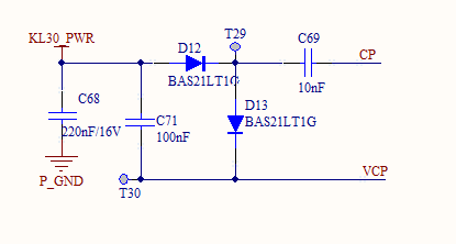
The Schematic like this,
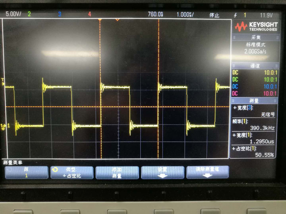
I use Oscilloscope test CP pins, the output single like this
I set Frequence = 0.52MHz, but output Frequence is 0.39MHz, the duty i set is 75%, but the output is 50%.
so i want to know how to correct it.
Thank you Very much.
已解决! 转到解答。
Hello,
The GDUCLK1 register is not for the Charge Pump but for the Boost Converter.
The Charge Pump Output Pin (CP) switches with 50% duty cycle and its frequency is configurable in the GDUCLK2 register.
Regards,
Daniel
Hello,
The GDUCLK1 register is not for the Charge Pump but for the Boost Converter.
The Charge Pump Output Pin (CP) switches with 50% duty cycle and its frequency is configurable in the GDUCLK2 register.
Regards,
Daniel

