- Forums
- Product Forums
- General Purpose MicrocontrollersGeneral Purpose Microcontrollers
- i.MX Forumsi.MX Forums
- QorIQ Processing PlatformsQorIQ Processing Platforms
- Identification and SecurityIdentification and Security
- Power ManagementPower Management
- MCX Microcontrollers
- S32G
- S32K
- S32V
- MPC5xxx
- Other NXP Products
- Wireless Connectivity
- S12 / MagniV Microcontrollers
- Powertrain and Electrification Analog Drivers
- Sensors
- Vybrid Processors
- Digital Signal Controllers
- 8-bit Microcontrollers
- ColdFire/68K Microcontrollers and Processors
- PowerQUICC Processors
- OSBDM and TBDML
- S32M
-
- Solution Forums
- Software Forums
- MCUXpresso Software and ToolsMCUXpresso Software and Tools
- CodeWarriorCodeWarrior
- MQX Software SolutionsMQX Software Solutions
- Model-Based Design Toolbox (MBDT)Model-Based Design Toolbox (MBDT)
- FreeMASTER
- eIQ Machine Learning Software
- Embedded Software and Tools Clinic
- S32 SDK
- S32 Design Studio
- GUI Guider
- Zephyr Project
- Voice Technology
- Application Software Packs
- Secure Provisioning SDK (SPSDK)
- Processor Expert Software
- MCUXpresso Training Hub
-
- Topics
- Mobile Robotics - Drones and RoversMobile Robotics - Drones and Rovers
- NXP Training ContentNXP Training Content
- University ProgramsUniversity Programs
- Rapid IoT
- NXP Designs
- SafeAssure-Community
- OSS Security & Maintenance
- Using Our Community
-
- Cloud Lab Forums
-
- Knowledge Bases
- ARM Microcontrollers
- i.MX Processors
- Identification and Security
- Model-Based Design Toolbox (MBDT)
- QorIQ Processing Platforms
- S32 Automotive Processing Platform
- Wireless Connectivity
- CodeWarrior
- MCUXpresso Suite of Software and Tools
- MQX Software Solutions
-
- Home
- :
- Product Forums
- :
- S12 / MagniV Microcontrollers
- :
- 9s12x ram decode
9s12x ram decode
- Subscribe to RSS Feed
- Mark Topic as New
- Mark Topic as Read
- Float this Topic for Current User
- Bookmark
- Subscribe
- Mute
- Printer Friendly Page
9s12x ram decode
- Mark as New
- Bookmark
- Subscribe
- Mute
- Subscribe to RSS Feed
- Permalink
- Report Inappropriate Content
Many years ago, I abandoned a project using an early 9s12xa512 uP. Recently I have started a new project using the 9s12xe uP and porting a good chunk of the original code. But I noticed a lot of the code is accessing the internal RAM using global instructions with GPAGE=0. I no longer have the original uP reference manual for the 9s12xa, but I remember the code working back then. The only explanation would be if somehow I knew that the internal RAM is replicated/duplicated as multiple images between 00_0000 and 0F_FFFF caused by incomplete decoding of the upper address lines. Does anyone know if this is the case?
Mike Huslig
- Mark as New
- Bookmark
- Subscribe
- Mute
- Subscribe to RSS Feed
- Permalink
- Report Inappropriate Content
Hi,the manual is still accessible on our pages..and attached. As you know the memory in the S12X devices is possible to be accessed by different ways either in 16 bit addressing mode or 24bit addressing mode where the paging is used.
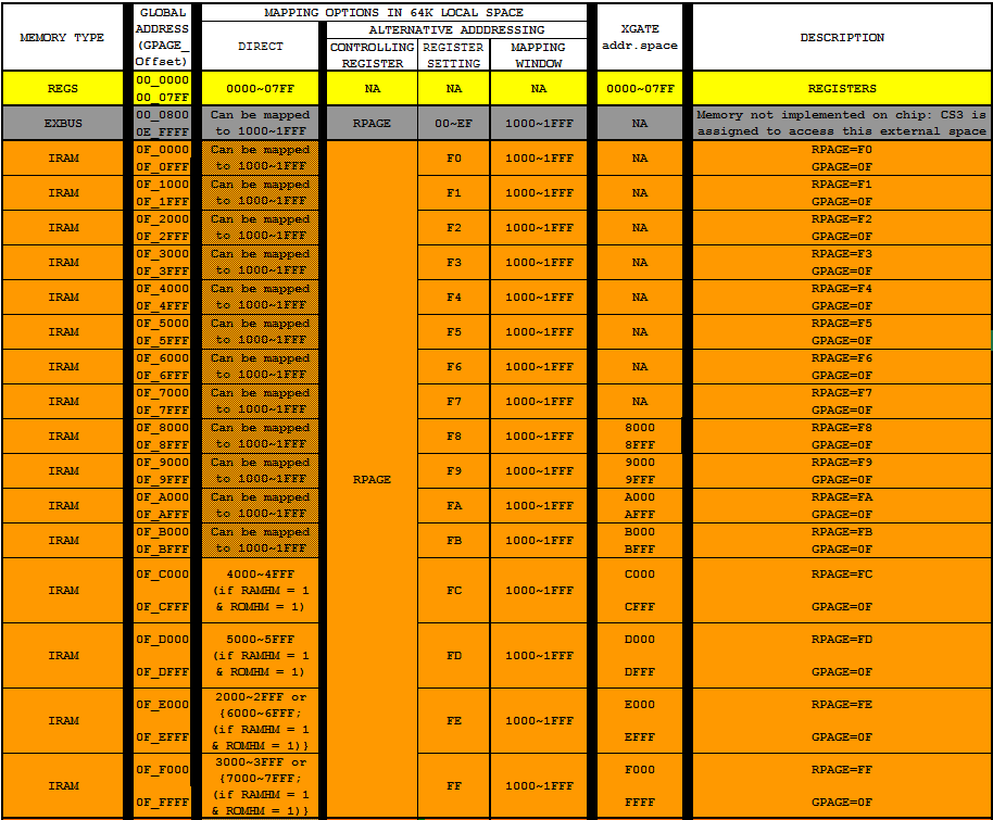
Gpage addrssing is able to cover entire address space of the MCU. Please look at the part of the memory map of the S12XE device...entire memory map is attached together with maps for mor S12XE devices. As you can see GPAGE 0 together with assemebler instructions for global load and global store accessing Register space and external memory space (external bus access, EBI module...https://community.nxp.com/docs/DOC-93594 ) in the case the device is used in expanded mode.....and no, there are not duplicated memory spaces. There is only a possibility to access one memory space in different ways.
Best regards,
Ladislav
- Mark as New
- Bookmark
- Subscribe
- Mute
- Subscribe to RSS Feed
- Permalink
- Report Inappropriate Content
Thank you. As usual I wasn't thinking it through. I was using CS3 to
access external RAM with GPAGE=0, not internal RAM. Sorry.
