- Forums
- Product Forums
- General Purpose MicrocontrollersGeneral Purpose Microcontrollers
- i.MX Forumsi.MX Forums
- QorIQ Processing PlatformsQorIQ Processing Platforms
- Identification and SecurityIdentification and Security
- Power ManagementPower Management
- MCX Microcontrollers
- S32G
- S32K
- S32V
- MPC5xxx
- Other NXP Products
- Wireless Connectivity
- S12 / MagniV Microcontrollers
- Powertrain and Electrification Analog Drivers
- Sensors
- Vybrid Processors
- Digital Signal Controllers
- 8-bit Microcontrollers
- ColdFire/68K Microcontrollers and Processors
- PowerQUICC Processors
- OSBDM and TBDML
- S32M
-
- Solution Forums
- Software Forums
- MCUXpresso Software and ToolsMCUXpresso Software and Tools
- CodeWarriorCodeWarrior
- MQX Software SolutionsMQX Software Solutions
- Model-Based Design Toolbox (MBDT)Model-Based Design Toolbox (MBDT)
- FreeMASTER
- eIQ Machine Learning Software
- Embedded Software and Tools Clinic
- S32 SDK
- S32 Design Studio
- GUI Guider
- Zephyr Project
- Voice Technology
- Application Software Packs
- Secure Provisioning SDK (SPSDK)
- Processor Expert Software
- MCUXpresso Training Hub
-
- Topics
- Mobile Robotics - Drones and RoversMobile Robotics - Drones and Rovers
- NXP Training ContentNXP Training Content
- University ProgramsUniversity Programs
- Rapid IoT
- NXP Designs
- SafeAssure-Community
- OSS Security & Maintenance
- Using Our Community
-
- Cloud Lab Forums
-
- Knowledge Bases
- ARM Microcontrollers
- i.MX Processors
- Identification and Security
- Model-Based Design Toolbox (MBDT)
- QorIQ Processing Platforms
- S32 Automotive Processing Platform
- Wireless Connectivity
- CodeWarrior
- MCUXpresso Suite of Software and Tools
- MQX Software Solutions
-
- Home
- :
- QorIQ Processing Platforms
- :
- QorIQ
- :
- Re: LS1043A and LS1046A - SerDes REF_CLK
LS1043A and LS1046A - SerDes REF_CLK
- Subscribe to RSS Feed
- Mark Topic as New
- Mark Topic as Read
- Float this Topic for Current User
- Bookmark
- Subscribe
- Mute
- Printer Friendly Page
- Mark as New
- Bookmark
- Subscribe
- Mute
- Subscribe to RSS Feed
- Permalink
- Report Inappropriate Content
Hello community,
i am working on a design with the LS1043A/46A processor. This processors should be exchangeable at one PCB-Design.
Is it needed to use all 4 SDx_REF_CLKx_P/N as input at the LS1046A or can i use the 2 SD1_REF_CLKx_P/N which the LS1043A provide.
Are the 4 SDx_REF_CLKx_P/N depend on anything while using all 8 SerDes-Lanes ?
For Example:
SD1_REF_CLK1_P/N is needed for Lane A-B (SerDes1) and SD1_REF_CLK2_P/N is needed for Lane C-D (SerDes1).
Or can i switch the REF_CLK ?
Thanks,
Best regards,
Juergen
Solved! Go to Solution.
- Mark as New
- Bookmark
- Subscribe
- Mute
- Subscribe to RSS Feed
- Permalink
- Report Inappropriate Content
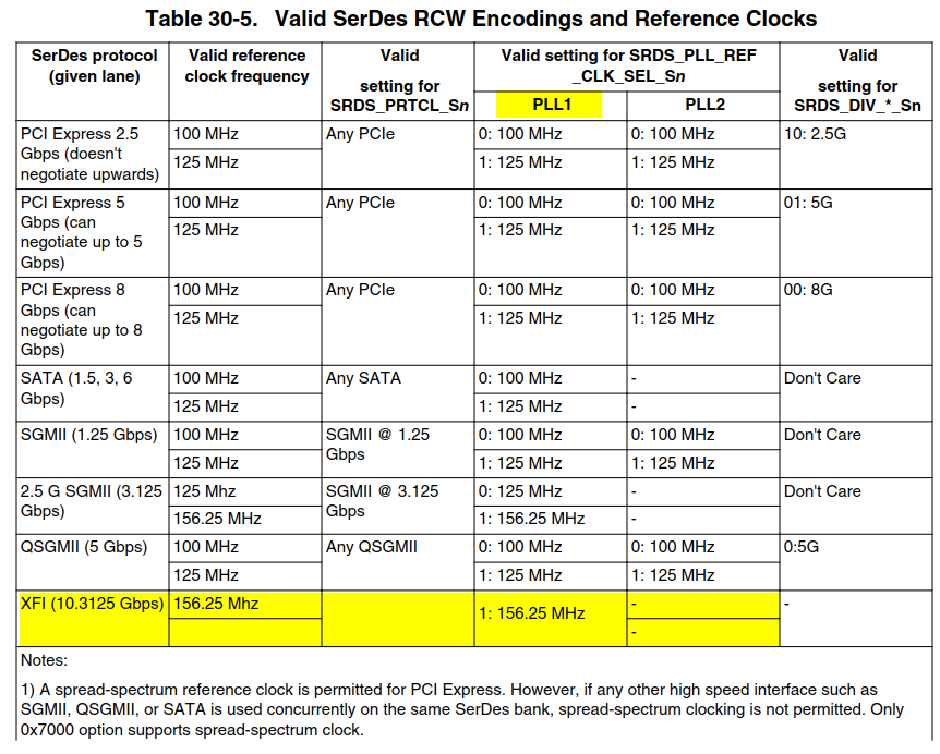
Note 2 and XFI clocking from PLL1 is incorrect in the Table 30-5.
Correct mapping is:
Lane Interface PLL-Mapping
D XFI 2
C XFI 2
B SGMII 1
A SGMII 1
- Mark as New
- Bookmark
- Subscribe
- Mute
- Subscribe to RSS Feed
- Permalink
- Report Inappropriate Content
Hi ufedor,
thanks for answering. Don't mind the question above, i had some wrong thoughts. I figured it out.
But i had another question:
This follow SerDes1 options shows the PLL-Mapping 2221 (XFI,XFI,SGMII,SGMII)
But the following note 2 says XFI can only be sourced from SerDes PLL1.
How can i understand that ?
Thanks,
Best regards,
Juergen
- Mark as New
- Bookmark
- Subscribe
- Mute
- Subscribe to RSS Feed
- Permalink
- Report Inappropriate Content
There is a typo in the note location marked yellow - correct is SerDes PLL2.
- Mark as New
- Bookmark
- Subscribe
- Mute
- Subscribe to RSS Feed
- Permalink
- Report Inappropriate Content
But table 30-5 says that XFI can only sourced from PLL1 (also note 2)
In table 30-1 the order of PLL assignment is wrong?
For Example RCW: 0x1133
Lane Interface PLL-Mapping
D XFI 2
C XFI 2
B SGMII 1
A SGMII 1
The right order should be:
Lane Interface PLL-Mapping
D XFI 1
C XFI 1
B SGMII 2
A SGMII 2
Is this correct, because i can't find the typo.
- Mark as New
- Bookmark
- Subscribe
- Mute
- Subscribe to RSS Feed
- Permalink
- Report Inappropriate Content
Note 2 and XFI clocking from PLL1 is incorrect in the Table 30-5.
Correct mapping is:
Lane Interface PLL-Mapping
D XFI 2
C XFI 2
B SGMII 1
A SGMII 1
- Mark as New
- Bookmark
- Subscribe
- Mute
- Subscribe to RSS Feed
- Permalink
- Report Inappropriate Content
Could anyone help me ?
- Mark as New
- Bookmark
- Subscribe
- Mute
- Subscribe to RSS Feed
- Permalink
- Report Inappropriate Content
PLLs used by specific protocols are shown in the processor's Reference Manuals:
LS1043A - Figure 32-1. Supported SerDes options, coulumn "PLL Napping"
LS1046A - Table 30-1. Supported SerDes1 options, column "PCIe Gen1/2 PLL Mapping"
The question is not clear because LS1043A has one SerDes, while LS1046A - two.
Please create a Technical Case so it will be possible to provide additional information concerning common board design:


