- Forums
- Product Forums
- General Purpose MicrocontrollersGeneral Purpose Microcontrollers
- i.MX Forumsi.MX Forums
- QorIQ Processing PlatformsQorIQ Processing Platforms
- Identification and SecurityIdentification and Security
- Power ManagementPower Management
- MCX Microcontrollers
- S32G
- S32K
- S32V
- MPC5xxx
- Other NXP Products
- Wireless Connectivity
- S12 / MagniV Microcontrollers
- Powertrain and Electrification Analog Drivers
- Sensors
- Vybrid Processors
- Digital Signal Controllers
- 8-bit Microcontrollers
- ColdFire/68K Microcontrollers and Processors
- PowerQUICC Processors
- OSBDM and TBDML
- S32M
-
- Solution Forums
- Software Forums
- MCUXpresso Software and ToolsMCUXpresso Software and Tools
- CodeWarriorCodeWarrior
- MQX Software SolutionsMQX Software Solutions
- Model-Based Design Toolbox (MBDT)Model-Based Design Toolbox (MBDT)
- FreeMASTER
- eIQ Machine Learning Software
- Embedded Software and Tools Clinic
- S32 SDK
- S32 Design Studio
- GUI Guider
- Zephyr Project
- Voice Technology
- Application Software Packs
- Secure Provisioning SDK (SPSDK)
- Processor Expert Software
- MCUXpresso Training Hub
-
- Topics
- Mobile Robotics - Drones and RoversMobile Robotics - Drones and Rovers
- NXP Training ContentNXP Training Content
- University ProgramsUniversity Programs
- Rapid IoT
- NXP Designs
- SafeAssure-Community
- OSS Security & Maintenance
- Using Our Community
-
- Cloud Lab Forums
-
- Knowledge Bases
- ARM Microcontrollers
- i.MX Processors
- Identification and Security
- Model-Based Design Toolbox (MBDT)
- QorIQ Processing Platforms
- S32 Automotive Processing Platform
- Wireless Connectivity
- CodeWarrior
- MCUXpresso Suite of Software and Tools
- MQX Software Solutions
-
- Home
- :
- トピック
- :
- NXP Designs ナレッジベース
- :
- Device-to-device communication via NFC demo
Device-to-device communication via NFC demo
- RSS フィードを購読する
- 新着としてマーク
- 既読としてマーク
- ブックマーク
- 購読
- 印刷用ページ
- 不適切なコンテンツを報告
Device-to-device communication via NFC demo
Device-to-device communication via NFC demo
This post entry provides a detailed description of how the Device-to-device communication demo was developed so that you can leverage this knowledge to integrate NFC into your own system. This document has been structured as follows:
Introduction
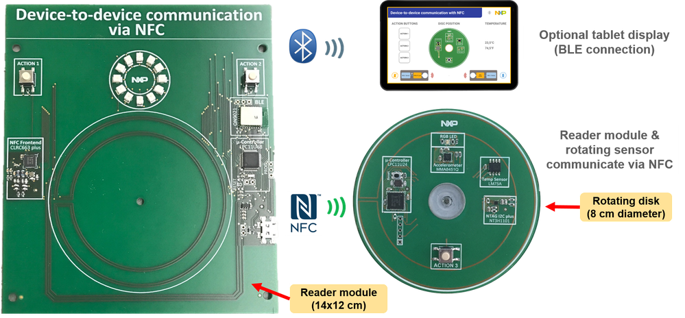
The Device-to-device communication demo shows how NFC can be used as a cable replacement between two units or devices. It is based on the CLRC663 plus NFC Frontend and the NTAG I2C plus connected tag solutions. It demonstrates how NFC is used for:
- Wireless communication with a batteryless unit.
- Wireless communication between two devices mounted in close vicinity that need to be completely isolated (e.g. dust or water proof).
- Wireless communication with a rotating part and as a cable replacement solution.
Device-to-device communication demo functionality
The purpose of the demo is to illustrate how to enable device-to-device communication via NFC. It consist of:
- A base board of 14x12 cm, which embeds the CLRC663 plus NFC reader IC for the RF field generation.
- A sensor embedded on a separate, rotating sensor disk of 8 cm diameter, which embeds the NTAG I2C plus connected tag.
The base board and the rotating sensor disk communicate via NFC and optionally, a tablet display can be connected via a Bluetooth Low Energy (BLE) connection (the BLE connection is beyond the scope of this post entry).
NFC for communication with a batteryless unit
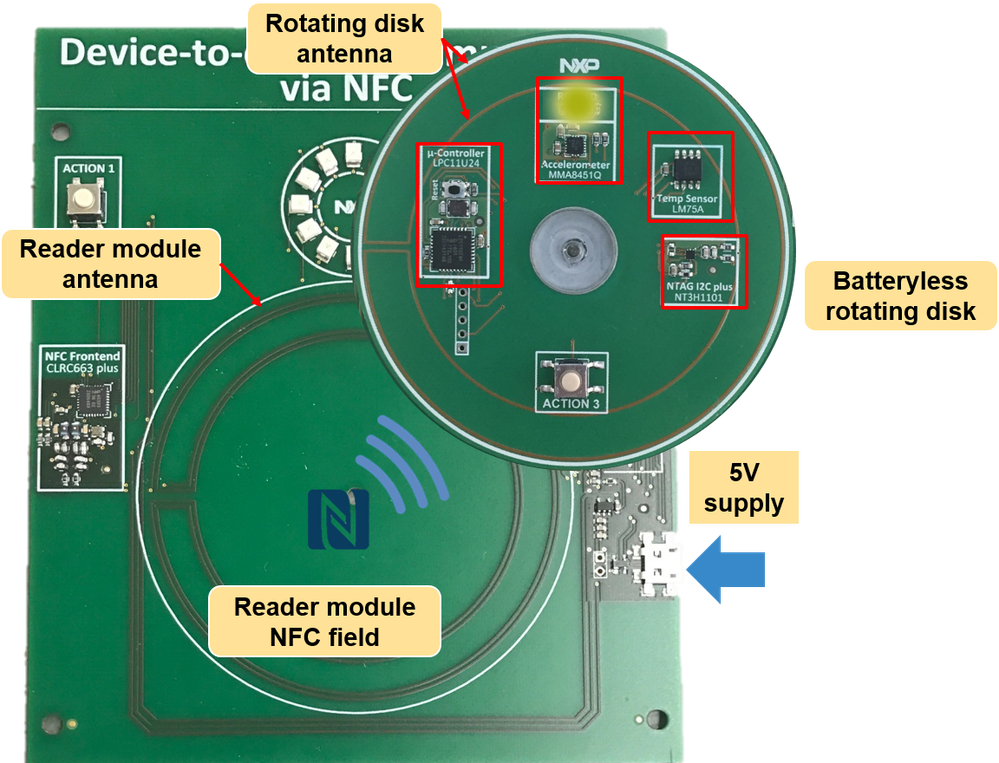
The first scenario demonstrates the use of NFC for communication with a batteryless unit or sensor. Energy from the RF field generated by an NFC reader can be harvested to power up small devices so that a battery or other power supply no longer needs to be included.
In this demo, only the base board is powered using a 5V supply input (e.g. USB battery bank) while the rotating disk electronics are powered using only the harvested energy from the RF field generated by the base board. To maximize energy transfer and avoid possible interference caused by the electronics, both the rotating disk and base board antennas are placed on the edges.
In the following video, you can observe how as soon as the base board is supplied, it starts generating an RF field and automatically. Then, all the electronics on the rotating disk are powered and its LED turns GREEN.
NFC for communication between two devices mounted in close proximity
The second scenario demonstrates the use of NFC for communication between two devices mounted in close proximity. For instance, any machine or device where sensors are inside or in close vicinity and the sensor needs to be completely sealed (e.g. waterproof, dustproof, etc).
In this demo, the bidirectional communication between the two units is demonstrated using push buttons, which light up LEDs on the opposite unit. For the base board to rotating disk communication direction:
- While action button 1 is pressed, the LED on the rotating disk turns BLUE.
- While action button 2 is pressed, the LED on the rotating disk turns RED.
- While action button 1 and button 2 are pressed, the LED on the rotating disk turns WHITE.
With the other way around, for the rotating disk to base board communication direction:
- While action button 3 is pressed, a pattern on the LED circle will appear.
NFC for communication with a rotating part as a cable replacement solution
The third and last scenario demonstrates the use of NFC to communicate wirelessly with two moving parts where cables may break. For instance, any solution consisting of a main unit and a sensing part recording mechanical-stress readings on moving parts.
In this demo, the accelerometer on the rotating disk continuously sends its coordinates to the base board, which lights up a specific LED according to the calculated angle between the two units. In the following video, you can see that the LED circle "follows" the movement of the rotating disk.
Hardware details
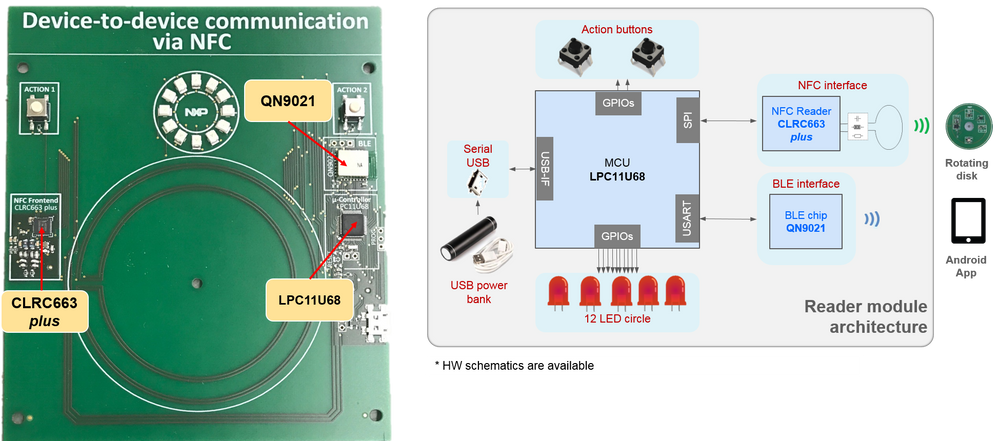
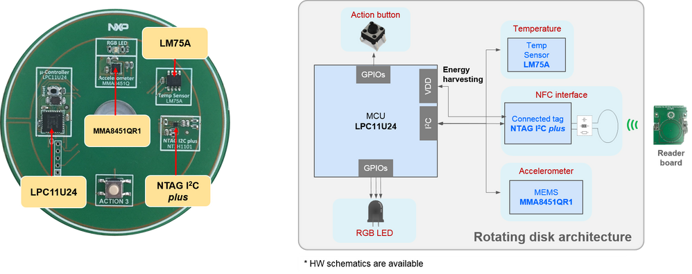
This section shows the architecture and main components of the base board and rotating disk. The PCB schematics are attached at the end of this post entry.
Base board based on CLRC663 plus
The disk has been dismounted so you can better appreciate the different components of the base board. The base board is driven by an LPC11U68 MCU, which is a low-cost Cortex-M0 USB solution, with 256 kB of flash memory, up to 80 GPIOs and several host interfaces (more details on the LPC11U68 product website).
From the LPC11U68 MCU, some of the GPIOs are used to connect the action buttons and the 12 LEDs of the circle, an SPI port is used to connect the CLRC663 plus NFC Frontend and, a USART port is used for connecting a BLE chip based on NXP's QN9021 chip.
The NFC functionality is provided by our CLRC663 plus reader IC, an NXP high performance multi-protocol reader. It is the evolution of CLRC663, with a larger LPCD detection range, more output power (2x times higher transmitter current), larger temperature operating range and pin-to-pin compatibility with the former version.
Rotating disk based on NTAG I2C plus
The rotating disk is based on NXP solutions as well. This PCB board is driven by an LPC11U24 MCU, which is a low-cost Cortex M0 32 bit MCU, with 32 kB of flash memory, up to 40 GPIOs and several host interfaces (more details on the LPC11U24 product website).
From the LPC11U24 MCU, some of the GPIOs are used to connect the action button 3 and the RGB LED. In addition, an I2C interface port is shared to connect a temperature sensor, the accelerometer and the NTAG I2C plus.
The NTAG I2C plus is a family of connected NFC tags that combines a memory, a passive NFC interface with a contact I2C interface. Functionally, the NTAG I2C plus behaves as a dual port memory. Therefore, the data can pass from an external NFC device to the embedded system. In addition, to this dual interface solution, it has more features:
- A field detection pin, to send a wake up signal
- The Energy harvesting, to power external devices
- The SRAM, a memory without writing cycles limitation
- The pass-through mode, for fast data exchange between interfaces
- Several memory access management settings from both NFC and I2C interfaces
- And an originality signature, to protect against clones.
Application logic
This section describes how data is exchanged between the reader module (base board) and the rotating disk using NTAG I2C plus as a bridge (pass-through mode) between the two embedded systems.
Reader module to rotating disk communication
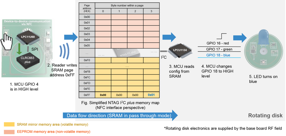
In this demo, the reader module sends data to the rotating disk when any of its two action buttons are pressed. The NTAG I2C plus is configured in pass-through mode and the SRAM memory is used as conduit between the twto units. The figure below illustrates a simplified representation of NTAG I2C plus memory seen from the NFC perspective (organized in pages of 4 bytes each). The red area represents the EEPROM memory while the yellow one represents the SRAM memory location. While the button 1 is pressed:
- The GPIO 4 of the LPC11U68 is in high level.
- The CLRC663 plus writes one byte into the SRAM memory (last page, value = 0x01).
- The LPC11U24 on the rotating disk reads the SRAM.
- The LPC11U24 changes the GPIO 18 status to high level.
- The RGB LED turns blue.
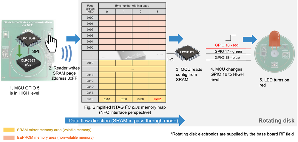
The operation that takes place while button 2 is pressed is pretty similar. Basically, it changes: the data written by the CLRC663 plus in the SRAM and the GPIO activated by the LPC11U24 on the rotating disk. More precisely, the steps are:
- The GPIO 5 of the LPC11U68 is in high level.
- The CLRC663 plus writes one byte into the SRAM memory (last page, value = 0x02).
- The LPC11U24 on the rotating disk reads the SRAM.
- The LPC11U24 changes the GPIO 16 status to high level and sets GPIO 18 to low level.
- The RGB LED turns red.
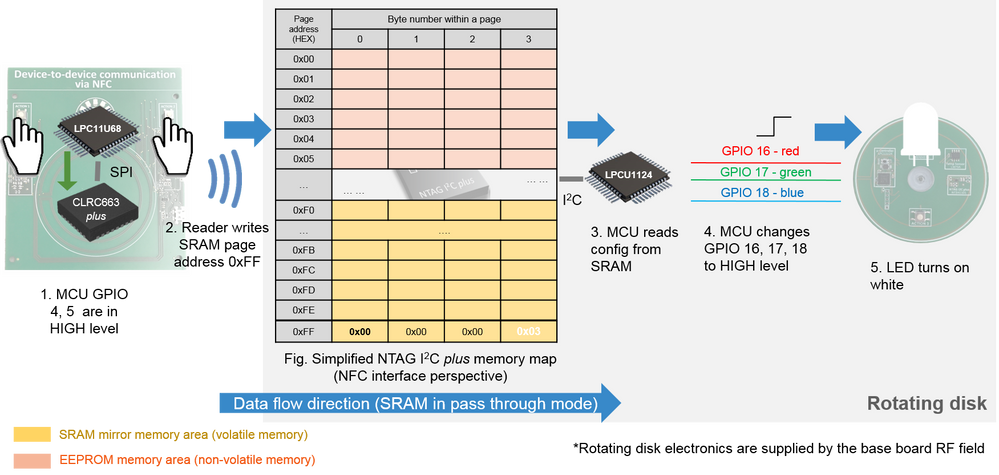
In the same way, while the two buttons are pressed at the same time:
- The LPC11U68 detects that GPIO 4 and 5 are in high level
- The CLRC663 plus programs a different value on the last SRAM byte (0x03).
- The LPC11U24 on the rotating disk reads the SRAM.
- The LPC11U24 sets to high the three GPIOs (16,17,18) controlling the RGB LED.
- The RGB LED turns white
The key message is that: what it is written in the SRAM controls the behavior of the rotating disk LED, demonstrating wireless data exchange between the two embedded systems.
Rotating disk to reader module communication
In this demo, the rotating disk keeps sending data to the reader module for as long as it is powered by the RF field. Precisely, it continuously sends the disk position (via the accelerometer axis coordinates) and the measured temperature value. Additionally, an extra byte is sent while the button 3 is pressed. The actual steps are:
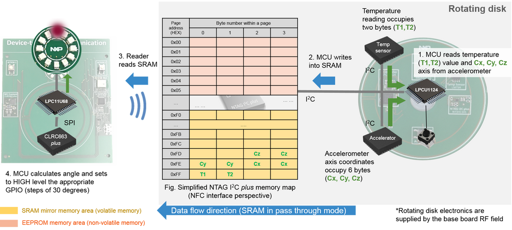
- First, the LPC11U24 MCU triggers a read operation to the temperature sensor and accelerometer. The temperaturre reading occupies 2 bytes while the accelerometer axis coordinates occupy 6 bytes. This data is transfered the LPC11U24 via the I2C shared bus.
- The LPC11U24 writes these 8 bytes into the SRAM in page addresses 0xFD, 0xFE and 0xFF (see the figure below).
- The CLRC663 plus reads the SRAM when the LPC11U24 has finished writing it.
- With the read information, the LPC11U68 base board MCU calculates the angle and sets the appropriate GPIO to high level. Since the LED circle contains 12 LEDs, the base board is able to represent position changes of 30 degrees (360º / 12 LEDs).
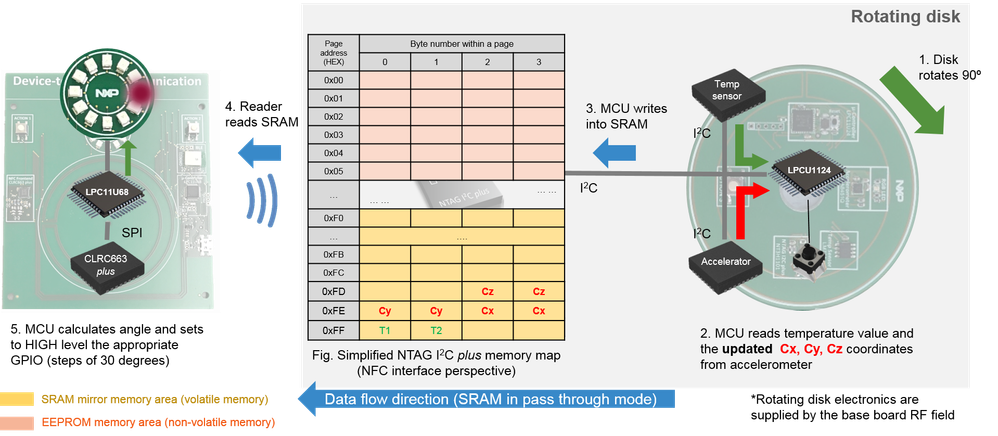
As mentioned, this data transfer keeps going for as long as the disk is powered. The key concept here is that the LED circle operation is directly controlled by the disk position and the axis coordinates which are exchanged via the NTAG I2C plus SRAM at any given moment. To illustrate this, the disk is rotated 90 º clockwise. The steps that take place are:
- The LPC11U24 MCU triggers the next reading command, the accelerometer axis coordinates have changed to different ones representing the new disk position (in red in the memory map figure below).
- The LPC11U24 writes into the SRAM again these 8 bytes (now with the updated accelerometer axis coordinates)
- The CLRC663 plus reads the SRAM when the LPC11U24 has finished writing it.
- With this new reading, the LPC11U68 MCU recalculates the angle and applies a different GPIO configuration (which leads to a different LED turned on in the circle).
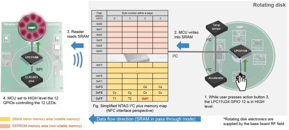
Last, while button 3 is pressed:
- The LPC11U24 GPIO 12 is set to high value.
- The LPC11U24 checks GPIO 12 pin status before writing into the SRAM. While it is high level, it adds an additional byte into the SRAM (third byte on page 0xFF- value=0x01).
- The CLRC663 plus reads the SRAM, getting the latest data from the moving part.
- With the current firmware, while the third byte on page address 0xFF is set to 0x01, the LPC11U68 performs a LED pattern activating all the GPIOs simultaneously (all the LEDs are ON).
MCU code details
This section explains the firmware implementation details for both the base board (CLRC663 plus) and the rotating disk (NTAG I2C plus). Before going into the firmware implementation details, a few considerations for data exchange synchronization when using the NTAG I2C plus pass-through mode are explained.
NTAG I2C plus pass-through mode data exchange synchronization considerations
In the demo, the pass-through mode is used to exchange data between the base board and the rotating disk. The pass-through mode provides the SRAM for data communication and the mechanisms for the synchronization of the data transfer. This signalling can be done through the field detection pin or by polling the equivalent registers over the I2C interface. For the NFC to I2C direction, the synchronization can be done:
- By checking the SRAM_I2C_READY register to learn if new data has been written by the RF interface.
- By checking the filed detection pin changing from HIGH to LOW voltage.
For I2C interface to NFC direction, the synchronization can be done:
- By checking the SRAM_RF_READY register to learn if new data has been written by the I2C interface.
- By checking the filed detection pin changing from LOW to HIGH voltage.
The following table includes register bits which can be used for communication synchronization. In addition, there is a dedicated application note providing more details on how NTAG I2C plus can be used for bidirectional data communication.
| Register bit | Use |
|---|---|
| PTHRU_ON_OFF | Detects if the pass-through mode is still enabled (gets reset in case of RF or I2C power down). |
| TRANSFER_DIR | Defines the data flow direction for the data transfer. |
| I2C_LOCKED | Detects if memory access is currently locked to I2C. |
| RF_LOCKED | Detects if Memory access is currently locked to RF. |
| SRAM_I2C_READY | Detects if there is data available in the SRAM buffer to be fetched by the I²C side. |
SRAM_RF_READY | Detects if there is data available in the SRAM buffer to be fetched by the RF interface. |
| RF_FIELD_PRESENT | Shows if a RF field strong enough to read the tag is there. |
Reader module MCU code
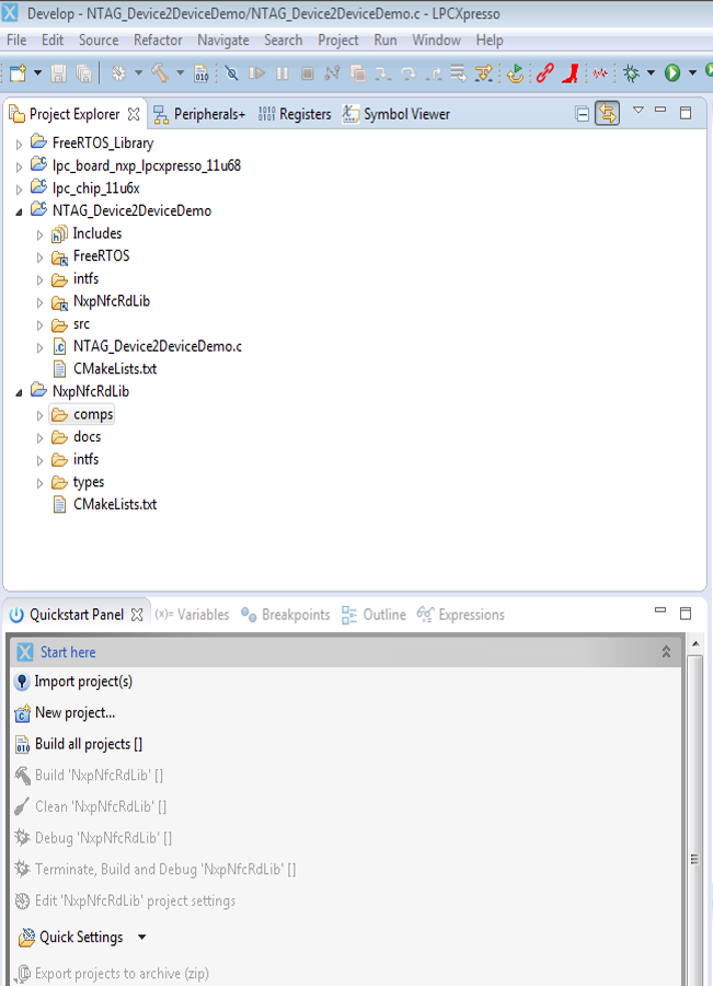
The MCU firmware was developed using our LPCXpresso platform, which provides a complete development environment for LPC MCU and LPC boards. In the source code, there are five project folders:
- The FreeRTOS project folder, which is an open source real-time operating system (RTOS) for embedded systems supporting many different architectures and compiler toolchains
- The Lpc_chip_11u6x_lib and nxp_lpcxpresso_11u68b project folders, which belong to the LPCOpen libraries supporting the LPC11U68 MCU and PCB board, the MCU chip integrated in the Explorer board. If you use another MCU, you should replace them by the specific LPCOpen libraries.
- The NTAG_Device2DeviceDemo project folder, which implements the logic supporting the device-to-device communication demo for the reader module.
- The NxpNfcRdLib project folder, which is the NXP's NFC Reader Library software stack supporting the implementation of the demo, the contactless protocols, the LPC MCU host interfaces and the CLRC663 drivers.
The reader module MCU code leverages on the NFC Reader Library. The NFC Reader Library is a software stack for creating and developing contactless applications for NXP's NFC readers. This API facilitates the most common operations required in NFC applications such as: reading or writing data into contactless cards, exchanging data with other NFC-enabled devices and emulating cards.
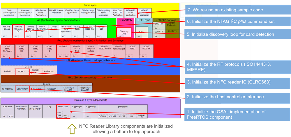
In order to use the NFC Reader Library, a stack of components has to be built up from the bottom to the top layer. Precisely, the application requirements define which modules need to be enabled and which do not. For the reader module firmware:
- The FreeRTOS is used.
- The SPI is used as host interface.
- A CLRC663 plus reader IC is used.
- And, communication with NTAG I2C plus is needed ( ISO14443 Type A card and NFC Forum Type 2 Tag compliant)
As a result, the software components that need to be enabled within the NFC Reader Library are depicted in the following picture:
NTAG_Device2DeviceDemo application workflow
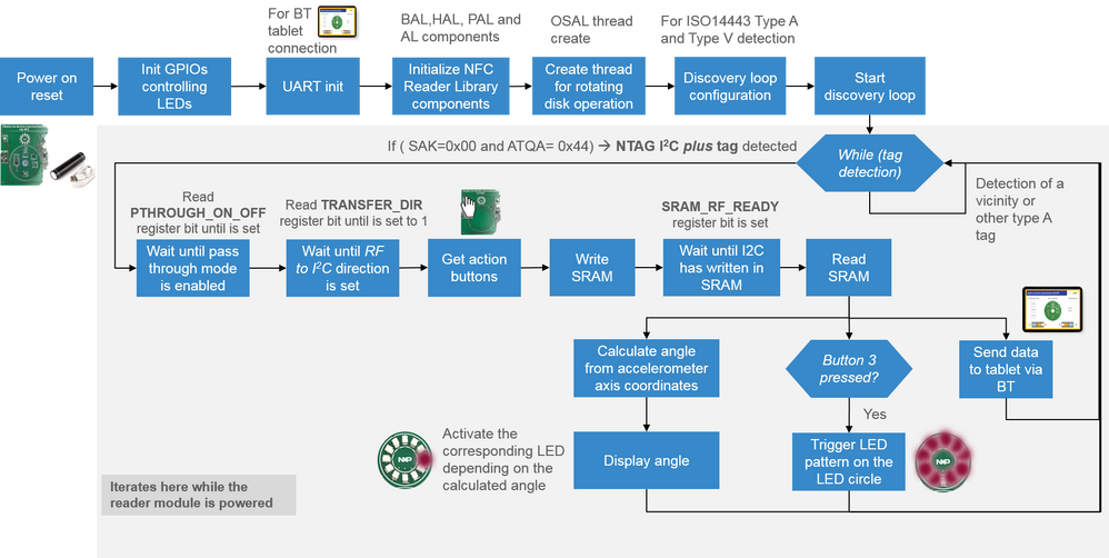
The reader module firmware starts its execution as soon as it is connected to the power bank. The firmware initializes the GPIOs, the UART for the tablet connection and the NFC Reader Library for the contactless operation. After all these initializations, the firmware code generates a new thread in charge of dealing with the disk operation. In this separate thread, the discovery loop for detection of Type A and Type V cards is configured and started. After that, the firmware keeps listening until the NTAG I2C plus is detected (i.e. the disk is mounted). On detection, the operation with the rotating disk starts:
- The reader module waits until the SRAM is available for the RF interface. The SRAM is available for the RF interface while the pass-through mode is enabled (PTHROUGH_ON_OFF register is set) and the RF to I2C direction is set (TRANSFER_DIR register bit).
- The board buttons are checked and the SRAM is written with the corresponding information.
At this point, the program awaits to receive data from the rotating disk. For that, it keeps polling if new data was written in the SRAM by the I2C interface (SRAM_RF_READY register bit is set). If new data is available, the SRAM is read and the data is processed:
- The accelerometer axis coordinates are read, the angle is calculated and the appropriate LED on the circle is activated.
- While the button 3 is pressed, the MCU triggers the LED pattern on the circle.
- Optionally, if the tablet connection is established, data is also sent using the BLE channel.
The following figure depicts the reader module application workflow in detail:
Rotating disk MCU code

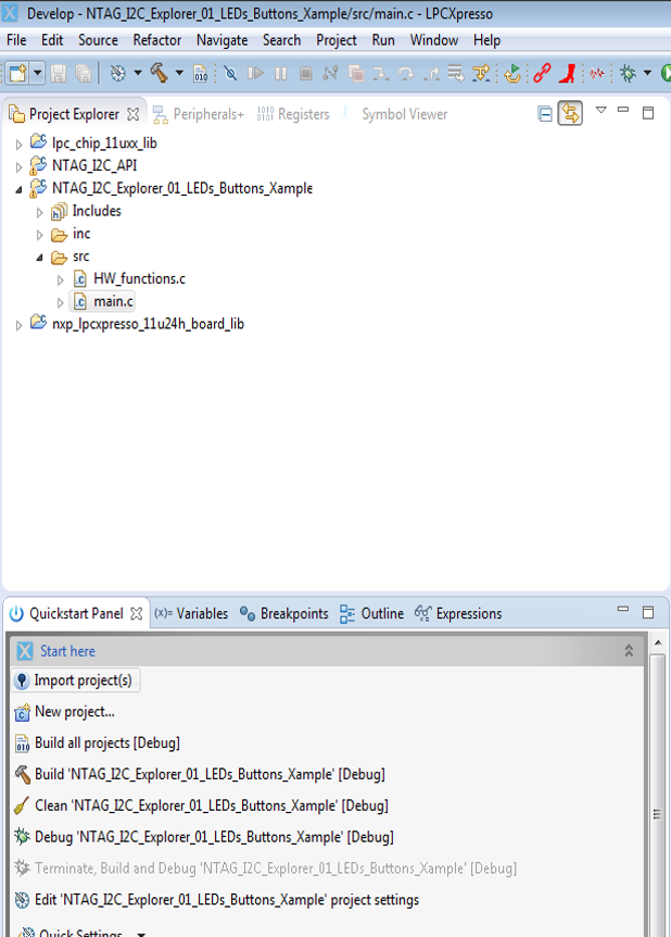
- The Lpc_chip_11uxx_lib and nxp_lpcxpresso_11u24h_board_lib project folders belong to the LPCOpen libraries supporting the LPC11U24 MCU and PCB board, the MCU chip integrated in the Explorer board. If you use another MCU, you should replace them by the specific LPCOpen libraries.
- The NTAG_I2C _API project folder is a library providing a set of functions and procedures that allow you to communicate with the NTAG I2C from the I2C interface. Among others, functions to perform memory operations on EEPROM, SRAM, registers and for enabling the pass through mode
- The NTAG_I2C _Explorer_01_LEDs_ButtonXample project folder implements the logic for the rotating disk of this demo.
NTAG_I2C _Explorer_01_LEDs_ButtonXample application workflow
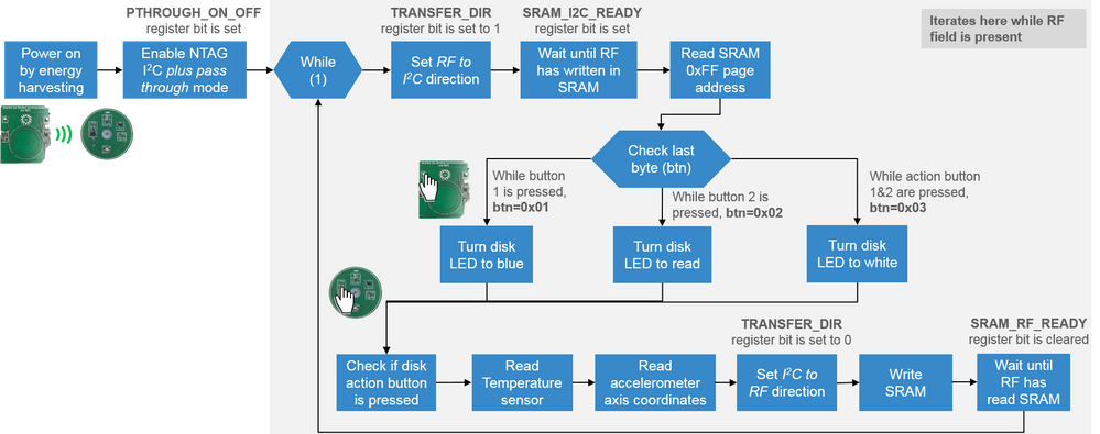
The rotating disk firmware starts its execution as soon as it harvests enough energy from the reader's module RF field. The first operation taken is to enable the pass-through mode. Then, the firmware stays on a loop for as long as it is energized.
In this loop, it sets the SRAM into RF to I2C direction (TRANSFER_DIR register bit) and waits until the base board has written data. After data has been written from the RF side, it reads the SRAM and checks the last byte:
- While the last byte value is 0x01, it means the button 1 is pressed and the firmware sets the RGB LED to blue
- While the last byte value is 0x02, it means the button 2 is pressed and the firmware sets the RGB LED to red
- While the last byte value is 0x03, it means the button 1 and 2 are pressed and the firmware sets the RGB LED to white.
After receiving data from the base board, it prepares to send data back. For that: it checks the button status, it reads the temperature value and the accelerometer position. Once all the data has been collected:
- It changes the SRAM to I2C to RF direction (TRANSFER_DIR register bit).
- It writes into the SRAM and waits until the RF has read the data (SRAM_RF_READY register is cleared).
This loop is repeated for as long as the disk is powered. The following figure depicts the rotating disk application workflow in detail:
Video recorded session
On 9 March 2017, a live session explaining the device-to-device communication demo was recorded. You can watch the recording here:
Available resources
Schematics
Please see attached in the separate attachment section below.
Device-to-device demo source code
Please see attached in the separate attachment section below.
Quick-start guide for showing the demo
Please see attached in the separate attachment section below
Android app
The android app can be used on a tablet or smart phone connected via BLE to this demo to show additional parameters, and to have a bigger screen for demonstrations. You find it in Google play ("device2devicedemo") and attached below.
- 既読としてマーク
- 新着としてマーク
- ブックマーク
- ハイライト
- 印刷
- 不適切なコンテンツを報告
Hi Jordi,
Thanks for demostration of device to device NFC communication.
What should be done to increase reading distance up to 30cm of reader module without increasing antenna diameter?
Can use of active tag instead of passive tag help to achieve this?
Regards
- 既読としてマーク
- 新着としてマーク
- ブックマーク
- ハイライト
- 印刷
- 不適切なコンテンツを報告
Hi,
The link http://nxp.com/assets/downloads/data/en/software/Device-to-Device-demo_SourceCode.zip does not seem to work for me, would it be possible to post a working link to the source.
Regards
- 既読としてマーク
- 新着としてマーク
- ブックマーク
- ハイライト
- 印刷
- 不適切なコンテンツを報告
Hi - just to let you know, we are working on getting the link back. Will take a few days.
- 既読としてマーク
- 新着としてマーク
- ブックマーク
- ハイライト
- 印刷
- 不適切なコンテンツを報告
Hi. The link continues to be broken. Any news on this?
How soon do you expect it to be back again?
Thanks
- 既読としてマーク
- 新着としてマーク
- ブックマーク
- ハイライト
- 印刷
- 不適切なコンテンツを報告
Hi Antonio and philipmcu (and all others who were looking for the source codes), as the link continues to be broken, I just posted the package as an attachment to this article. I hope this helps. Please share your application if possible - I'm curious, and I hope this inspires others as well.
