- Forums
- Product Forums
- General Purpose MicrocontrollersGeneral Purpose Microcontrollers
- i.MX Forumsi.MX Forums
- QorIQ Processing PlatformsQorIQ Processing Platforms
- Identification and SecurityIdentification and Security
- Power ManagementPower Management
- MCX Microcontrollers
- S32G
- S32K
- S32V
- MPC5xxx
- Other NXP Products
- Wireless Connectivity
- S12 / MagniV Microcontrollers
- Powertrain and Electrification Analog Drivers
- Sensors
- Vybrid Processors
- Digital Signal Controllers
- 8-bit Microcontrollers
- ColdFire/68K Microcontrollers and Processors
- PowerQUICC Processors
- OSBDM and TBDML
- S32M
-
- Solution Forums
- Software Forums
- MCUXpresso Software and ToolsMCUXpresso Software and Tools
- CodeWarriorCodeWarrior
- MQX Software SolutionsMQX Software Solutions
- Model-Based Design Toolbox (MBDT)Model-Based Design Toolbox (MBDT)
- FreeMASTER
- eIQ Machine Learning Software
- Embedded Software and Tools Clinic
- S32 SDK
- S32 Design Studio
- GUI Guider
- Zephyr Project
- Voice Technology
- Application Software Packs
- Secure Provisioning SDK (SPSDK)
- Processor Expert Software
- MCUXpresso Training Hub
-
- Topics
- Mobile Robotics - Drones and RoversMobile Robotics - Drones and Rovers
- NXP Training ContentNXP Training Content
- University ProgramsUniversity Programs
- Rapid IoT
- NXP Designs
- SafeAssure-Community
- OSS Security & Maintenance
- Using Our Community
-
- Cloud Lab Forums
-
- Knowledge Bases
- ARM Microcontrollers
- i.MX Processors
- Identification and Security
- Model-Based Design Toolbox (MBDT)
- QorIQ Processing Platforms
- S32 Automotive Processing Platform
- Wireless Connectivity
- CodeWarrior
- MCUXpresso Suite of Software and Tools
- MQX Software Solutions
-
- Home
- :
- 本人確認とセキュリティ
- :
- NFC
- :
- Re: TDA8035HN Footprint Question
TDA8035HN Footprint Question
- RSS フィードを購読する
- トピックを新着としてマーク
- トピックを既読としてマーク
- このトピックを現在のユーザーにフロートします
- ブックマーク
- 購読
- ミュート
- 印刷用ページ
TDA8035HN Footprint Question
- 新着としてマーク
- ブックマーク
- 購読
- ミュート
- RSS フィードを購読する
- ハイライト
- 印刷
- 不適切なコンテンツを報告
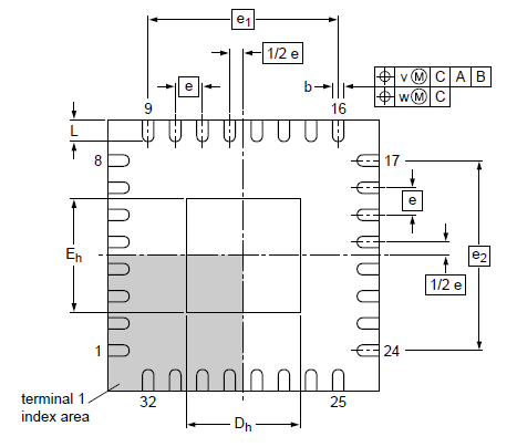
We are layout a PCB incorporating TDA8035HN. The package outline suggests there's a metal paddle in the center, but there's no mention of connection or recommended PCB footprint. Is the square depicted by dimensions Dh and Eh a metal pad? Can this be ignored?
-Mark
- 新着としてマーク
- ブックマーク
- 購読
- ミュート
- RSS フィードを購読する
- ハイライト
- 印刷
- 不適切なコンテンツを報告
Hi Mark,
QFN/SON are designed with the die attach pad exposed at the bottom side to create an efficient heat path to the PCB. Heat transfer can be further facilitated by metal vias in the thermal land pattern of the PCB. The exposed pad also enables ground connection.
It is not necessary to solder this part, but it improves and optimizes thermal performance.
Here is an application note that explains the above with great detail.
Assembly guidelines for QFN (quad flat no-lead) and SON (small outline no-lead) packages
Please let me know if you have any further questions.
Have a great day!
Sabina
- 新着としてマーク
- ブックマーク
- 購読
- ミュート
- RSS フィードを購読する
- ハイライト
- 印刷
- 不適切なコンテンツを報告
Thank you.
Missing from the TDA8035 datasheet:
- Can this pad be connected to the ground plane?
- No specifications for thermal impedance, i.e. ThetaJC, etc.
- Ptot listed at 0.45W. Is this maximum package dissipation, or expected power consumption?
-Mark
- 新着としてマーク
- ブックマーク
- 購読
- ミュート
- RSS フィードを購読する
- ハイライト
- 印刷
- 不適切なコンテンツを報告
Hi Mark,
Here are the answer to your questions:
1. As mentioned in the last post it is not necessary, but it can be connected to ground. Connecting it will , enhance the thermal and electrical performance of the package. For details of the PCB footrprint size and recommendations you can check section 4.2.2.1 of the document attached in the above post.
2. Unfortunately the specific Junction-to-case value is not available, the data sheet only provides the junction-to-ambient value.
3. This is the total dissipation, in other words its the power lost through heat. Please note here, that these values were tested in controlled laboratory environments with the chip by itself.
Please let me know if you have any further questions.
Best Regards,
Sabina
