- Forums
- Product Forums
- General Purpose MicrocontrollersGeneral Purpose Microcontrollers
- i.MX Forumsi.MX Forums
- QorIQ Processing PlatformsQorIQ Processing Platforms
- Identification and SecurityIdentification and Security
- Power ManagementPower Management
- MCX Microcontrollers
- S32G
- S32K
- S32V
- MPC5xxx
- Other NXP Products
- Wireless Connectivity
- S12 / MagniV Microcontrollers
- Powertrain and Electrification Analog Drivers
- Sensors
- Vybrid Processors
- Digital Signal Controllers
- 8-bit Microcontrollers
- ColdFire/68K Microcontrollers and Processors
- PowerQUICC Processors
- OSBDM and TBDML
- S32M
-
- Solution Forums
- Software Forums
- MCUXpresso Software and ToolsMCUXpresso Software and Tools
- CodeWarriorCodeWarrior
- MQX Software SolutionsMQX Software Solutions
- Model-Based Design Toolbox (MBDT)Model-Based Design Toolbox (MBDT)
- FreeMASTER
- eIQ Machine Learning Software
- Embedded Software and Tools Clinic
- S32 SDK
- S32 Design Studio
- GUI Guider
- Zephyr Project
- Voice Technology
- Application Software Packs
- Secure Provisioning SDK (SPSDK)
- Processor Expert Software
- MCUXpresso Training Hub
-
- Topics
- Mobile Robotics - Drones and RoversMobile Robotics - Drones and Rovers
- NXP Training ContentNXP Training Content
- University ProgramsUniversity Programs
- Rapid IoT
- NXP Designs
- SafeAssure-Community
- OSS Security & Maintenance
- Using Our Community
-
- Cloud Lab Forums
-
- Knowledge Bases
- ARM Microcontrollers
- i.MX Processors
- Identification and Security
- Model-Based Design Toolbox (MBDT)
- QorIQ Processing Platforms
- S32 Automotive Processing Platform
- Wireless Connectivity
- CodeWarrior
- MCUXpresso Suite of Software and Tools
- MQX Software Solutions
-
- Home
- :
- 本人確認とセキュリティ
- :
- NFC
- :
- SLRC61003 Schematics design question
SLRC61003 Schematics design question
- RSS フィードを購読する
- トピックを新着としてマーク
- トピックを既読としてマーク
- このトピックを現在のユーザーにフロートします
- ブックマーク
- 購読
- ミュート
- 印刷用ページ
SLRC61003 Schematics design question
- 新着としてマーク
- ブックマーク
- 購読
- ミュート
- RSS フィードを購読する
- ハイライト
- 印刷
- 不適切なコンテンツを報告
Customer is designing schematics using SLRC61003,there are two questions.
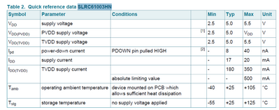
1 Their MCU power supply voltage is 2.5V,so they power VDD,PVDD and TVDD of SLRC61003 with 2.5V.I see the lower limit of these power is 2.5V in datasheet. Are there some potential risks for this design?
2 For TDO,TDI,TMS and TCK pins, If they don't use,how to deal with?Floating or Grounding?I find in demo design TDI,TMS and TCK are gounding and TDO is floating.
I attach the schematic file,please help check.
- 新着としてマーク
- ブックマーク
- 購読
- ミュート
- RSS フィードを購読する
- ハイライト
- 印刷
- 不適切なコンテンツを報告
Hi Bob,
See below, please!
>>1 Their MCU power supply voltage is 2.5V,so they power VDD,PVDD and TVDD of SLRC61003 with 2.5V.I see the lower limit of these power is 2.5V in datasheet. Are there some potential risks for this design?
For SLRC61003HN, min voltage is no problem.
In theory, there is no risk, but TVDD=2.5V, this voltage is relatively low, which will have an impact on the transmit power.
2 For TDO,TDI,TMS and TCK pins, If they don't use,how to deal with?Floating or Grounding?I find in demo design TDI,TMS and TCK are gounding and TDO is floating.
---You can design according to the method of DEMO board.
---In fact, there is no problem with these pins floating.
[Note]
checked your schematic, no other issues were found.
Hope this information is helpful to you.
Have a nice day!
B.R,
Weidong
