- Forums
- Product Forums
- General Purpose MicrocontrollersGeneral Purpose Microcontrollers
- i.MX Forumsi.MX Forums
- QorIQ Processing PlatformsQorIQ Processing Platforms
- Identification and SecurityIdentification and Security
- Power ManagementPower Management
- Wireless ConnectivityWireless Connectivity
- RFID / NFCRFID / NFC
- Advanced AnalogAdvanced Analog
- Neural Processing UnitsNeural Processing Units
- MCX Microcontrollers
- S32G
- S32K
- S32V
- MPC5xxx
- Other NXP Products
- S12 / MagniV Microcontrollers
- Powertrain and Electrification Analog Drivers
- Sensors
- Vybrid Processors
- Digital Signal Controllers
- 8-bit Microcontrollers
- ColdFire/68K Microcontrollers and Processors
- PowerQUICC Processors
- OSBDM and TBDML
- S32M
- S32Z/E
-
- Solution Forums
- Software Forums
- MCUXpresso Software and ToolsMCUXpresso Software and Tools
- CodeWarriorCodeWarrior
- MQX Software SolutionsMQX Software Solutions
- Model-Based Design Toolbox (MBDT)Model-Based Design Toolbox (MBDT)
- FreeMASTER
- eIQ Machine Learning Software
- Embedded Software and Tools Clinic
- S32 SDK
- S32 Design Studio
- GUI Guider
- Zephyr Project
- Voice Technology
- Application Software Packs
- Secure Provisioning SDK (SPSDK)
- Processor Expert Software
- Generative AI & LLMs
-
- Topics
- Mobile Robotics - Drones and RoversMobile Robotics - Drones and Rovers
- NXP Training ContentNXP Training Content
- University ProgramsUniversity Programs
- Rapid IoT
- NXP Designs
- SafeAssure-Community
- OSS Security & Maintenance
- Using Our Community
-
- Cloud Lab Forums
-
- Knowledge Bases
- ARM Microcontrollers
- i.MX Processors
- Identification and Security
- Model-Based Design Toolbox (MBDT)
- QorIQ Processing Platforms
- S32 Automotive Processing Platform
- Wireless Connectivity
- CodeWarrior
- MCUXpresso Suite of Software and Tools
- MQX Software Solutions
- RFID / NFC
- Advanced Analog
- Neural Processing Units
-
- NXP Tech Blogs
- Home
- :
- RFID / NFC
- :
- NFC
- :
- PN5180 power consumption problem
PN5180 power consumption problem
オプション
- RSS フィードを購読する
- トピックを新着としてマーク
- トピックを既読としてマーク
- このトピックを現在のユーザーにフロートします
- ブックマーク
- 購読
- ミュート
- 印刷用ページ
PN5180 power consumption problem
10-15-2019
03:20 AM
2,988件の閲覧回数

lu_xzh
Contributor I
- 新着としてマーク
- ブックマーク
- 購読
- ミュート
- RSS フィードを購読する
- ハイライト
- 印刷
- 不適切なコンテンツを報告
Hello everyone:
I have a problem about PN5180.I hope you can help me,thank you
My question is below:
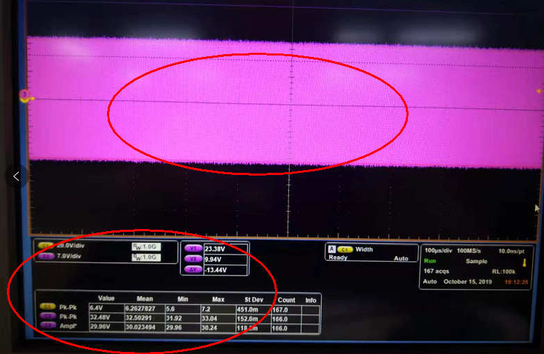
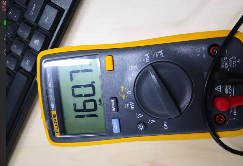
When the current consumption is 160mA, I use an oscilloscope to observe the antenna terminal voltage is only 32.48V,
Why is the power consumption so high and the antenna terminal voltage so low
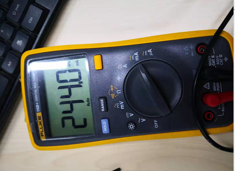
Another question,Put the card on the coil and the power consumption reaches 244mA
The power consumption Shouldn't be lower when the card is on the coil?
Best Wishes
2 返答(返信)
10-16-2019
08:44 PM
2,902件の閲覧回数

 fangfang
NXP TechSupport
- 新着としてマーク
- ブックマーク
- 購読
- ミュート
- RSS フィードを購読する
- ハイライト
- 印刷
- 不適切なコンテンツを報告
Hello,
In order to better service for you would you please introduce the steps of testing you did, then I may replicate the phenomenon on my site.
10-16-2019
10:54 PM
2,902件の閲覧回数
lu_xzh
Contributor I
- 新着としてマーク
- ブックマーク
- 購読
- ミュート
- RSS フィードを購読する
- ハイライト
- 印刷
- 不適切なコンテンツを報告
你好:
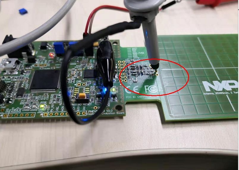
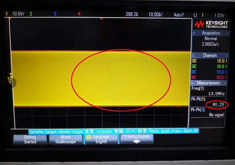
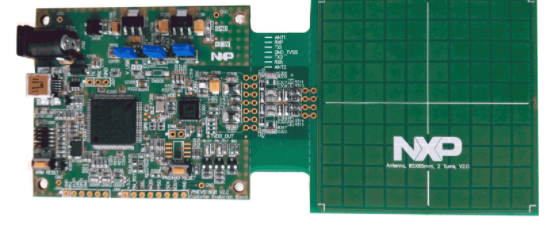
1、使用下面的板子,测试位置为发射端(图中红圈),使用示波器观察这儿的波形大小,测试峰峰值是40V,测试ITVDD功耗是160mA
Use the board below, the test position is the transmitting end (red circle in the figure), use the oscilloscope to observe the waveform size here, the test peak-peak value is 40V, and the test ITVDD power consumption is 160mA
我们之前测试别的芯片,测试发射端波形大小基本会有80V以上(TVDD功耗没有我们现在的大),这个波形峰值小的原因是因为DPC的因素吗?还是说本来就这么大,发射场强与这个发射端的峰值有直接的关系吗
We have tested other chips before, and the waveform size of the test transmitter will basically be over 80V (TVDD power consumption is not as large as our current power). Is the reason for the small peak value of this waveform due to DPC? Or is there a direct relationship between the intensity of the field and the peak at this end
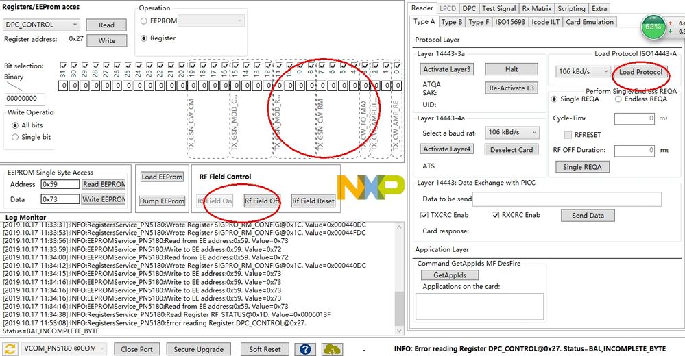
2、DPC的功能也不是很清楚,所谓的动态功率控制,是不是我放卡在不同的位置,都会保持场强在一个合适的值,不是说过来或者过小。DPC验证的话,通过TVDD或者发射端峰值波形可以看出来什么变化吗
The function of DPC is not very clear, the so-called dynamic power control, whether I put the card in different positions, will keep the field strength in a suitable value, not to say come over or too small. If DPC is verified, what changes can be seen through TVDD or peak waveform at the transmitting end
谢谢
thank you