- Forums
- Product Forums
- General Purpose MicrocontrollersGeneral Purpose Microcontrollers
- i.MX Forumsi.MX Forums
- QorIQ Processing PlatformsQorIQ Processing Platforms
- Identification and SecurityIdentification and Security
- Power ManagementPower Management
- MCX Microcontrollers
- S32G
- S32K
- S32V
- MPC5xxx
- Other NXP Products
- Wireless Connectivity
- S12 / MagniV Microcontrollers
- Powertrain and Electrification Analog Drivers
- Sensors
- Vybrid Processors
- Digital Signal Controllers
- 8-bit Microcontrollers
- ColdFire/68K Microcontrollers and Processors
- PowerQUICC Processors
- OSBDM and TBDML
- S32M
-
- Solution Forums
- Software Forums
- MCUXpresso Software and ToolsMCUXpresso Software and Tools
- CodeWarriorCodeWarrior
- MQX Software SolutionsMQX Software Solutions
- Model-Based Design Toolbox (MBDT)Model-Based Design Toolbox (MBDT)
- FreeMASTER
- eIQ Machine Learning Software
- Embedded Software and Tools Clinic
- S32 SDK
- S32 Design Studio
- GUI Guider
- Zephyr Project
- Voice Technology
- Application Software Packs
- Secure Provisioning SDK (SPSDK)
- Processor Expert Software
- MCUXpresso Training Hub
-
- Topics
- Mobile Robotics - Drones and RoversMobile Robotics - Drones and Rovers
- NXP Training ContentNXP Training Content
- University ProgramsUniversity Programs
- Rapid IoT
- NXP Designs
- SafeAssure-Community
- OSS Security & Maintenance
- Using Our Community
-
- Cloud Lab Forums
-
- Knowledge Bases
- ARM Microcontrollers
- i.MX Processors
- Identification and Security
- Model-Based Design Toolbox (MBDT)
- QorIQ Processing Platforms
- S32 Automotive Processing Platform
- Wireless Connectivity
- CodeWarrior
- MCUXpresso Suite of Software and Tools
- MQX Software Solutions
-
Dear experts:
I'm porting a boot-loader works well on MPC5642A to MPC5644A (based on C90FL SDD)
The document UM_C90FL_MM_JDP_SSD.pdf is my reference.
Now, my question is the flashing failed at block address 0x80000.
The difference is: this block is defined as High-address block0 (H0) in 5642A, but it is defined as Low-address Block 0 (L0)Flash B in 5644A. same difference for block address 0xC0000
My question is about how to set correct pramater value for C90FL SDD API functions
1)In page17, function GetLock(), parameter blkLockIndicator, LOCK_LOW_PRIMARY/LOCK_LOW_SECONDARY PRIMARY means Flash A? and SECONDARY means Flash B?
2)For page 11, function FlashErase(), how to set parameter lowEnabledBlocks value for block addess 0x80000 (L0 of flash B)? because there is also a L0 in Flash A.
3)Also, how to set parameter midEnabledBlocks: value for block address 0xC0000 (M0 of Flash A)?
4)Page 7 and 8, could you please confirm the block index should follow logical address mapping?
5) For 5642A , there is same block numbering principle for physical and logical address? As those in Table11-1 of 5642 UM?
Another question is: Is there a register telling me the MCU is 5642A or 5644A?
Following is my debug snapshot while writing flash
I'm very sorry the source code is forbidden to be uploaded to the public forum according to Company policy..
If necessary, it can be sent to your email box.
thanks and BR
YiChuan
已解决! 转到解答。
Hi YiChuan,
first of all, I will mention (maybe for others) that there are two versions of the driver:
for MPC5642A:
https://www.nxp.com/webapp/Download?colCode=C90FL_SM_JDP_FLASH_SSD_DEVD
for MPC5644A:
https://www.nxp.com/webapp/Download?colCode=MPC5644A_C90FL_SSD_DEVD
The drivers are not compatible, it is a must to use the correct one.
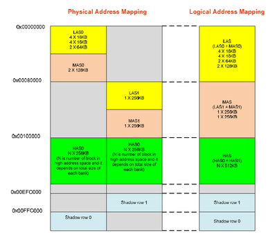
In case of MPC5644A, it's necessary to use logical address mappping. Do not consider that there are flash block A and flash block B. When using the driver, this is not important anymore, consider the flash as one flash block.
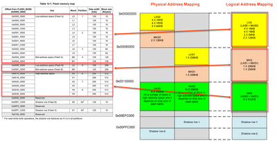
That also means Table 12-1 in the reference manual is not valid here. The relation between physical mapping and logical mapping is like this:
Example: 256KB block at 0x8_0000 is not low block now, it's first middle block. When you are going to unlock this block or select this block for erase, you should use bit 0 for middle blocks.
I believe the picture above should solve all your troubles.
To check which MCU you have, read SIU_MIDR register.
Regards,
Lukas


