- Forums
- Product Forums
- General Purpose MicrocontrollersGeneral Purpose Microcontrollers
- i.MX Forumsi.MX Forums
- QorIQ Processing PlatformsQorIQ Processing Platforms
- Identification and SecurityIdentification and Security
- Power ManagementPower Management
- Wireless ConnectivityWireless Connectivity
- RFID / NFCRFID / NFC
- MCX Microcontrollers
- S32G
- S32K
- S32V
- MPC5xxx
- Other NXP Products
- S12 / MagniV Microcontrollers
- Powertrain and Electrification Analog Drivers
- Sensors
- Vybrid Processors
- Digital Signal Controllers
- 8-bit Microcontrollers
- ColdFire/68K Microcontrollers and Processors
- PowerQUICC Processors
- OSBDM and TBDML
- S32M
-
- Solution Forums
- Software Forums
- MCUXpresso Software and ToolsMCUXpresso Software and Tools
- CodeWarriorCodeWarrior
- MQX Software SolutionsMQX Software Solutions
- Model-Based Design Toolbox (MBDT)Model-Based Design Toolbox (MBDT)
- FreeMASTER
- eIQ Machine Learning Software
- Embedded Software and Tools Clinic
- S32 SDK
- S32 Design Studio
- GUI Guider
- Zephyr Project
- Voice Technology
- Application Software Packs
- Secure Provisioning SDK (SPSDK)
- Processor Expert Software
-
- Topics
- Mobile Robotics - Drones and RoversMobile Robotics - Drones and Rovers
- NXP Training ContentNXP Training Content
- University ProgramsUniversity Programs
- Rapid IoT
- NXP Designs
- SafeAssure-Community
- OSS Security & Maintenance
- Using Our Community
-
- Cloud Lab Forums
-
- Knowledge Bases
- ARM Microcontrollers
- i.MX Processors
- Identification and Security
- Model-Based Design Toolbox (MBDT)
- QorIQ Processing Platforms
- S32 Automotive Processing Platform
- Wireless Connectivity
- CodeWarrior
- MCUXpresso Suite of Software and Tools
- MQX Software Solutions
-
- Home
- :
- Product Forums
- :
- MPC5xxx
- :
- Re: question about MPC5744p Flex_PWM output trigger
question about MPC5744p Flex_PWM output trigger
- Subscribe to RSS Feed
- Mark Topic as New
- Mark Topic as Read
- Float this Topic for Current User
- Bookmark
- Subscribe
- Mute
- Printer Friendly Page
question about MPC5744p Flex_PWM output trigger
- Mark as New
- Bookmark
- Subscribe
- Mute
- Subscribe to RSS Feed
- Permalink
- Report Inappropriate Content
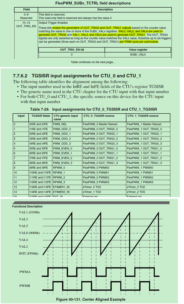
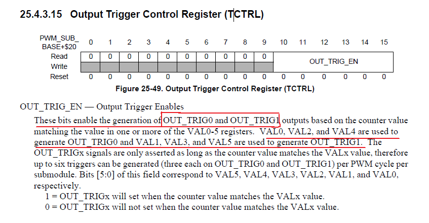
VAL0, VAL2, and VAL4 are used to generate OUT_TRIG0 and VAL1, VAL3, and VAL5 are used to generate OUT_TRIG1. what does that mean?
As i understand,
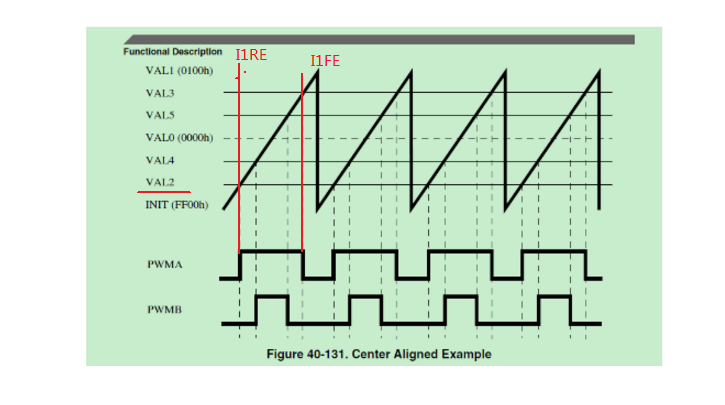
Sub0_VAL2 will generate OUT_TRIG0_0 riseEdge(I1RE), Sub0_VAL3 will generate OUT_TRIG0_0 fallEdge(I1FE).
Sub0_VAL4 will generate OUT_TRIG1_0 riseEdge(I5RE), Sub0_VAL5 will generate OUT_TRIG1_0 fallEdge(I5FE),
Sub1_VAL2 will generate OUT_TRIG0_1 riseEdge(I2RE), Sub0_VAL3 will generate OUT_TRIG0_1 fallEdge(I2FE).
Sub1_VAL4 will generate OUT_TRIG1_1 riseEdge(I6RE), Sub0_VAL5 will generate OUT_TRIG1_1 fallEdge(I6FE),
Sub0_VAL0 will generate PWMX0 riseEdge(I9RE), Sub0_VAL1 will generate PWMX0 fallEdge(I9FE).
Sub1_VAL0 will generate PWMX1 riseEdge(I10RE), Sub0_VAL1 will generate PWMX0 fallEdge(I10FE).
Do i understand correct? thank you very much!
- Mark as New
- Bookmark
- Subscribe
- Mute
- Subscribe to RSS Feed
- Permalink
- Report Inappropriate Content
thank you for Petr & Yanna!
- Mark as New
- Bookmark
- Subscribe
- Mute
- Subscribe to RSS Feed
- Permalink
- Report Inappropriate Content
Hi,
I hope this figure could help you.
Yanna
- Mark as New
- Bookmark
- Subscribe
- Mute
- Subscribe to RSS Feed
- Permalink
- Report Inappropriate Content
Yanna,
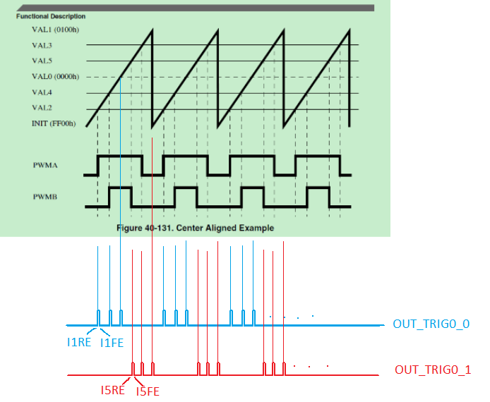
you are not correct. Here is a graphic explanation how OUT_TRIGx_y signals are generated. Here submodule's 0 OUT_TRIG0_0/OUT_TRIG0_1 signals are assumed and SUB0.TCTRL = 0x3F (all compare registers generate trigger pulse).
Petr
- Mark as New
- Bookmark
- Subscribe
- Mute
- Subscribe to RSS Feed
- Permalink
- Report Inappropriate Content
Petr thank you very much!
i still have 4 questions:
Q1: if i chose pwmx0 as the ctu tgsisr source(I9RE or I9FE =1), when does the signal pwmx0 happen(val0---> riseEdge & fallEdge?)? can you graphic for me? thank you very much!
Q2: if i want to use out_trig0_0 as the source, according to your graphic, val0/2/4 will all generate out_trig0_0, but i only want to use val2 generate the signal. So do i need to set a special value to val0/4 in order to avoid generate out_trig0_0 signal?
Q3: if i want to use out_trig1_0 as the source, according to your graphic, val1/3/5 will all generate out_trig1_0, but i only want to generate one pulse in a pwm period. So i no choice except for val1(val1 determins the period), is that correect?
Q4: if i set val0=val2=val4(or val1=val3=val5), i can get only one pulse(out_trigx_0) in a pwm period, is that correct?
- Mark as New
- Bookmark
- Subscribe
- Mute
- Subscribe to RSS Feed
- Permalink
- Report Inappropriate Content
A1) The PWMX generation is closely related to submodule period. The PWM signals are generated in the following manner.
- The INIT and VAL1 registers define the PWM modulo/period. So the PWM counter counts from INIT to VAL1 and then reinit to INIT again etc.
- The VAL2 resp. VAL3 define the compare value when PWMA goes High resp. Low.
- The VAL4 resp. VAL5 define the compare value when PWMB goes High resp. Low.
- The VAL0 defines half cycle reload point and also define the time when PWMX signal is set and the local sync signal is reset.
- The VAL1 also causes PWMX reseting and asserting local sync.
So the usage of PMWA and PWMB signals is easy. The PWMX, if not use as input (for capture feature etc), can generate also the PWM signal but you have to take into account that it represents the local sync signal, which is usually selected as sync source by INIT_SEL bits of CTRL2.
The OCTRL’s POLA, POLB, POLX bits inverts PWMA, PWMB and PWMX polarity.
A2) just set TCTRL = 0x04; // VAL2 match generate OUT_TRIG0
A3) not sure which “match” you want to use, so lets say VAL3, then
just set TCTRL = 0x08; // VAL3 match generate OUT_TRIG1
A4) VALx registers does not enable OUT_TRIG generation, it just defines a position in PWM period when OUT_TRIG pulse is generated if enabled by TCTRL.
Petr
- Mark as New
- Bookmark
- Subscribe
- Mute
- Subscribe to RSS Feed
- Permalink
- Report Inappropriate Content
Hi,
My understanding is belove.
Q1:
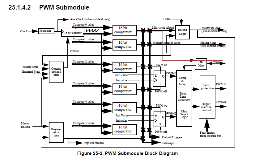
If you select PWMX for output pin, then it is high or low should be determined by Val0 register.
Following is a figure from MPC5643L RM.
Q2&Q3&Q4: You can select the signal (Val0 or Val2 or Val4) to out_trig0_0 signal by configuring TCTRLregister.
Yanna
- Mark as New
- Bookmark
- Subscribe
- Mute
- Subscribe to RSS Feed
- Permalink
- Report Inappropriate Content
Hi,Peter
I remember that there exists the register which determine out signal high or low when the counter matches the Valx value.
So my original understanding is that Rising and Falling edge signal cann't be selected at the same time.
a few minutes ago, I searched the register , but I cann't find it. is my undrstanding wrong?
I use MPC5643L.
Thanks very much!
Yanna
- Mark as New
- Bookmark
- Subscribe
- Mute
- Subscribe to RSS Feed
- Permalink
- Report Inappropriate Content
Hi,Petr
Yes,you are right.I have know it.
My understanding : Using rising or falling edge is determined by certain register. I1Re and I1Fe cann't happen at the same time.
Thanks very much!
Yanna
- Mark as New
- Bookmark
- Subscribe
- Mute
- Subscribe to RSS Feed
- Permalink
- Report Inappropriate Content
yes this is what i think! thank you very much
- Mark as New
- Bookmark
- Subscribe
- Mute
- Subscribe to RSS Feed
- Permalink
- Report Inappropriate Content
:smileyhappy:
- Mark as New
- Bookmark
- Subscribe
- Mute
- Subscribe to RSS Feed
- Permalink
- Report Inappropriate Content
Hi,
With the help of the TCTRL you define whether and which compare of VALx register generates the OUT_TRIG0 and OUT_TRIG1 output signals which go to the CTU. The connection of OUT_TRIG0 and OUT_TRIG1 signals to CTU is shown in the Figure 7-9 and the Table 7-29;
It is in the format OUT_TRIGx_y
the Y means the FlexPWM submodule, There are four submodules on FlexPWM (0,1,2 and 3).
The X shows it is either OUT_TRIG0 or OUT_TRIG1 signal.
You may see equivalent PWM_ODD_Y and PWM_EVEN_Y signals (Y corresponds to submodule number). Thus you can match OUT_TRIGX_Y (VAL0/1/2/3/4/5) with bits 14-29 in TGSISR register.
Master Reload and OUT_TRIGx_y signals are generated as very short pulse signal, so the rising and falling edge selection may looks little bit irrelevant. Rising/falling edge selection is more applicable for rest of trigger sources (PWMXn, eTIMER output and external pin).
BR, Petr
- Mark as New
- Bookmark
- Subscribe
- Mute
- Subscribe to RSS Feed
- Permalink
- Report Inappropriate Content
hi, Petr, thank you for your replying!
what i want to know is "VAL0, VAL2, and VAL4 are used to generate OUT_TRIG0",
how out_trig0 can be generated by val0/2/4, can you Draw a diagram for this?
PS: i think na yan's answer is right.
if na yan's answer is right, OUT_TRIG0 is generated by val2/3(not val0/2/4), OUT_TRIG1 is generated by val4/5(not by val1/3/5)

