- Forums
- Product Forums
- General Purpose MicrocontrollersGeneral Purpose Microcontrollers
- i.MX Forumsi.MX Forums
- QorIQ Processing PlatformsQorIQ Processing Platforms
- Identification and SecurityIdentification and Security
- Power ManagementPower Management
- Wireless ConnectivityWireless Connectivity
- RFID / NFCRFID / NFC
- MCX Microcontrollers
- S32G
- S32K
- S32V
- MPC5xxx
- Other NXP Products
- S12 / MagniV Microcontrollers
- Powertrain and Electrification Analog Drivers
- Sensors
- Vybrid Processors
- Digital Signal Controllers
- 8-bit Microcontrollers
- ColdFire/68K Microcontrollers and Processors
- PowerQUICC Processors
- OSBDM and TBDML
- S32M
-
- Solution Forums
- Software Forums
- MCUXpresso Software and ToolsMCUXpresso Software and Tools
- CodeWarriorCodeWarrior
- MQX Software SolutionsMQX Software Solutions
- Model-Based Design Toolbox (MBDT)Model-Based Design Toolbox (MBDT)
- FreeMASTER
- eIQ Machine Learning Software
- Embedded Software and Tools Clinic
- S32 SDK
- S32 Design Studio
- GUI Guider
- Zephyr Project
- Voice Technology
- Application Software Packs
- Secure Provisioning SDK (SPSDK)
- Processor Expert Software
-
- Topics
- Mobile Robotics - Drones and RoversMobile Robotics - Drones and Rovers
- NXP Training ContentNXP Training Content
- University ProgramsUniversity Programs
- Rapid IoT
- NXP Designs
- SafeAssure-Community
- OSS Security & Maintenance
- Using Our Community
-
- Cloud Lab Forums
-
- Knowledge Bases
- ARM Microcontrollers
- i.MX Processors
- Identification and Security
- Model-Based Design Toolbox (MBDT)
- QorIQ Processing Platforms
- S32 Automotive Processing Platform
- Wireless Connectivity
- CodeWarrior
- MCUXpresso Suite of Software and Tools
- MQX Software Solutions
-
Rslv Resolver ADC sampling synchronization
Hello Guys
Recently I am studying NXP application note AN3943, RSLV resolver driver application note.
There is one point that I am not quite understand:
How to synchronize the ADC trigger signal that can make sure the ADC samples at the peak point of the resolver analog reference signal?
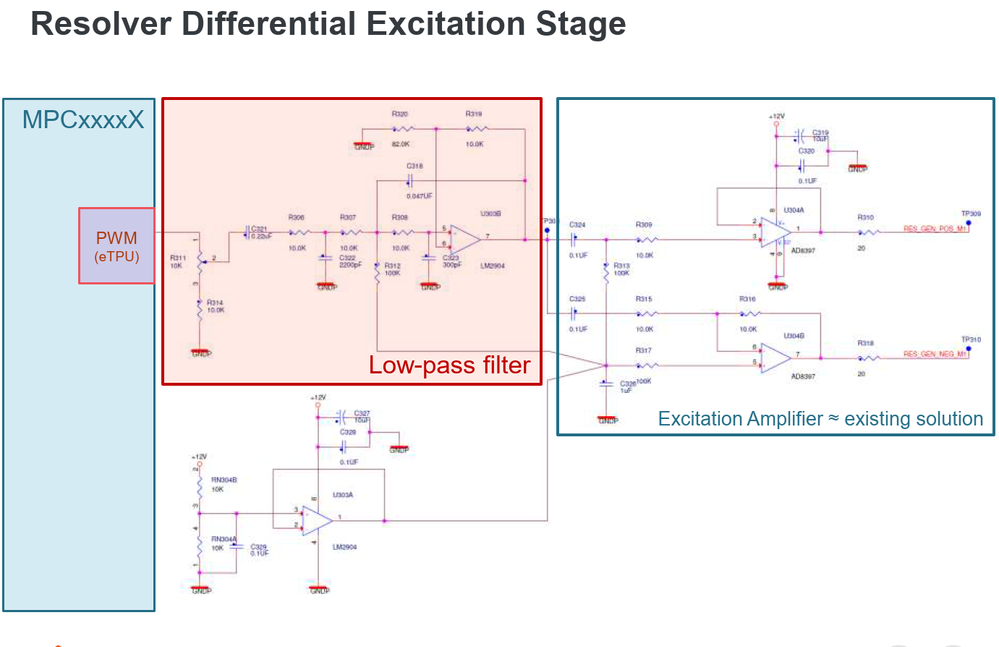
From the diagram (Figure 9), I can see there are resolver digital reference and resolver analog reference (this should be the excitation signal). So in my understanding, the resolver digital reference is generated by the eTPU PWM function, so what is the relationship between the resolver digital reference and resolver analog reference? I am a little bit confused about that. How to configure this PWM output and the ADC trigger PWM from the eTPU to make sure the synchronization?
I attached both screenshots of the diagram.
Thanks a lot for your help
Ni
Hi, there is a hardware interface in between like this:
AN3943 references AN1942/D describing Resolver theory and hardware interface as well:
https://www.nxp.com/docs/en/application-note/AN1942.pdf
Hope it helps
