- Forums
- Product Forums
- General Purpose MicrocontrollersGeneral Purpose Microcontrollers
- i.MX Forumsi.MX Forums
- QorIQ Processing PlatformsQorIQ Processing Platforms
- Identification and SecurityIdentification and Security
- Power ManagementPower Management
- MCX Microcontrollers
- S32G
- S32K
- S32V
- MPC5xxx
- Other NXP Products
- Wireless Connectivity
- S12 / MagniV Microcontrollers
- Powertrain and Electrification Analog Drivers
- Sensors
- Vybrid Processors
- Digital Signal Controllers
- 8-bit Microcontrollers
- ColdFire/68K Microcontrollers and Processors
- PowerQUICC Processors
- OSBDM and TBDML
- S32M
-
- Solution Forums
- Software Forums
- MCUXpresso Software and ToolsMCUXpresso Software and Tools
- CodeWarriorCodeWarrior
- MQX Software SolutionsMQX Software Solutions
- Model-Based Design Toolbox (MBDT)Model-Based Design Toolbox (MBDT)
- FreeMASTER
- eIQ Machine Learning Software
- Embedded Software and Tools Clinic
- S32 SDK
- S32 Design Studio
- GUI Guider
- Zephyr Project
- Voice Technology
- Application Software Packs
- Secure Provisioning SDK (SPSDK)
- Processor Expert Software
- MCUXpresso Training Hub
-
- Topics
- Mobile Robotics - Drones and RoversMobile Robotics - Drones and Rovers
- NXP Training ContentNXP Training Content
- University ProgramsUniversity Programs
- Rapid IoT
- NXP Designs
- SafeAssure-Community
- OSS Security & Maintenance
- Using Our Community
-
- Cloud Lab Forums
-
- Knowledge Bases
- ARM Microcontrollers
- i.MX Processors
- Identification and Security
- Model-Based Design Toolbox (MBDT)
- QorIQ Processing Platforms
- S32 Automotive Processing Platform
- Wireless Connectivity
- CodeWarrior
- MCUXpresso Suite of Software and Tools
- MQX Software Solutions
-
- Home
- :
- Product Forums
- :
- MPC5xxx
- :
- MPA5643L_eDMA
MPA5643L_eDMA
- Subscribe to RSS Feed
- Mark Topic as New
- Mark Topic as Read
- Float this Topic for Current User
- Bookmark
- Subscribe
- Mute
- Printer Friendly Page
- Mark as New
- Bookmark
- Subscribe
- Mute
- Subscribe to RSS Feed
- Permalink
- Report Inappropriate Content
I think the code (AN4794) exists some errors..
Q1:Dma.c
about the DMA channel 1, there exist following codes,
EDMA.CHANNEL[1].TCDWORD20_.B.CITER_E_LINK = 1; // link to channel 0 on minor loop
EDMA.CHANNEL[1].TCDWORD20_.B.CITER_LINKCH = 0; //
EDMA.CHANNEL[1].TCDWORD28_.B.BITER_E_LINK = 0; // no link on minor loop
EDMA.CHANNEL[1].TCDWORD28_.B.BITER_LINKCH = 0;
In general ,we should configure the citer_e_link bit value equal to the biter_e_link bit value ,also citer_e_linkch and biter_e_linkch ,ortherwise a configuration error will be reported.
My confusion is from the corresponding technical report(AN4794), the result is normal , but we can get some information from RM(reference mannul), following is the description of the biter_e_link,
“This is the initial value copied into the citer.e_link field when the major loop is completed. The citer.e_link field controls channel linking during channel execution.” From this,we can get if the maior loop is completed,then the the citer_e_link bit value will be decided by the biter_e_link bit value.
If so,after completing one maior loop, then the citer.e_link will becmome 0 ,the case is in direct contradiction to the principle the author proposed. I can’t understand how he could get the right result,is my understanding wrong?
Thanks very much!
Yanna
Original Attachment has been moved to: dma.c.zip
Original Attachment has been moved to: AN4794SW.zip
Solved! Go to Solution.
- Mark as New
- Bookmark
- Subscribe
- Mute
- Subscribe to RSS Feed
- Permalink
- Report Inappropriate Content
Hi,
smod creates circular buffer. It says how many LSB bits are used to increment the address. Upper bits in address remain untouched.
Example (1):
SADDR = 0x4000_0000
SOFF = 1
SMOD = 1 //only the last bit in address is touched when address is incremented
If more than two bytes are going to be transferred, following addresses will be used:
0x4000_0000
0x4000_0001
0x4000_0000
0x4000_0001
...
Example (2):
SADDR = 0x4000_0000
SOFF = 1
SMOD = 2 //only two last bits in address are touched when address is incremented
If more than four bytes are going to be transferred, following addresses will be used:
0x4000_0000
0x4000_0001
0x4000_0002
0x4000_0003
0x4000_0000
0x4000_0001
0x4000_0002
0x4000_0003
...
If smod/dmod is used (different from 0) then saddr/daddr should be aligned accordingly. For example, if smod=3 then saddr should be aligned to 8 bytes.
Lukas
- Mark as New
- Bookmark
- Subscribe
- Mute
- Subscribe to RSS Feed
- Permalink
- Report Inappropriate Content
Q3:Priority
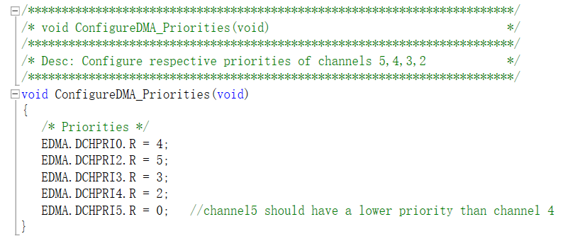
In An4794, the author said that The DMA transfer for the force-out configuration should have the highest priority over other DMA transfers., that means , the channel 0 and 1 should have the higher priority over the channel 4 and 5. But in codes,the author violate the priciple.
Thanks very much!
Yanna
- Mark as New
- Bookmark
- Subscribe
- Mute
- Subscribe to RSS Feed
- Permalink
- Report Inappropriate Content
I will ping Yves if he can comment...
- Mark as New
- Bookmark
- Subscribe
- Mute
- Subscribe to RSS Feed
- Permalink
- Report Inappropriate Content
- Mark as New
- Bookmark
- Subscribe
- Mute
- Subscribe to RSS Feed
- Permalink
- Report Inappropriate Content
Hello Yanna,
You are right, there are a few typos in the note and in the code itself.
Regarding the eDMA channel 1:
channel 1 should be configured to link to channel 0 on minor loop, and to not link on major loop. The code actually configured a link to channel 0 on *major* loop, and no link on minor loop (the inconsistent setting of biter_e_linkch=0 and citer_e_linkch=1 results in no link on minor loop). It still worked in spite of this mistake because it only caused a shift of one channel1 transfer.
Regarding the DMA priority:
Small mistake there, as the DMA channel priorities only affect the behaviour of the DMA when there are some concurrent requests, which is not the case here because all DMA requests are time-triggered. I will change the code to this configuration:
ConfigureDMA_Priorities(void) {
/* Priorities */
DCHPRI0.R = 4;
DCHPRI1.R = 3;
DCHPRI2.R = 5;
DCHPRI3.R = 2;
DCHPRI4.R = 1;
DCHPRI5.R = 0; //channel5 should have a lower priority than channel 4
}
Regarding the note itself:
I realize that the table 1 pages 11-12 has a lot of typos, I should correct the values of the offsets and of the source size.
I will try to have a new revision of the note published on nxp.com. I will keep you informed.
Thank you for looking so carrefully at my application note, you are a fantastic reviewer !
- Mark as New
- Bookmark
- Subscribe
- Mute
- Subscribe to RSS Feed
- Permalink
- Report Inappropriate Content
Hi, Yves
Thanks for your reply! Your application note help me a lot for understanding the basic consepts about FlexPWM and CTU and DMA .
I think a good review should be someone who propose valuable ideas other than point out some small typos. :smileyhappy:
I have another question about DMA_MUX source.
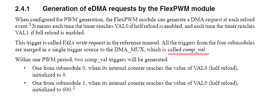
In AN4794, when the counter reach the value of VAL0(SUB0 and SUB1 of FlexPWM_0), a DMA transfer will occur.(configure FlexPWM registers ) So the corresponding DMA source bit equal 12(comp_val).
My understanding is if we set the VALDE bit and configure the DMA channel source equal 12 (enable DMA,) then the counter reach the value of VALx(x=0,1,2,3,4,5),a DMA transfer will occur. Is it right?
FLEXPWM_0.SUB[0].DMAEN.B.VALDE = 1; //Enable DMA
DMAMUX.CHCONFIG[1].B.SOURCE = 12; //FlexPWM write request
If it is right, then the VAL2(3…) register not only VAL0 cause a DMA transfer, is it right?
But from the waveform of AN4794, we can know that the DMA transfer occur only when the counter reach the VAL0 value, did there exist the register which select the VALx write request to the comp_val signal?
Addition: Strictly, if a DMA transfer occur when FIFO 0 contains 4 ADC results, then FIFO 0 threthold should be 0x3. Is it right?
Thanks very much!
Yanna
- Mark as New
- Bookmark
- Subscribe
- Mute
- Subscribe to RSS Feed
- Permalink
- Report Inappropriate Content
Hi Yanna,
Regarding the DMA triggers by the FlexPWM:
In the chapter 2.4.1, the AN describes shortly when the FlexPWM can trigger a DMA transfer. Basically, a DMA transfer can be triggered at each reload event, ie when the submodule's counter reaches the value of VAL0 (=half reload, because VAL0 is "traditionnaly" 0, ie in the middle of the PWM period) and/or VAL1 (=full reload because this events occurs at the end of the PWM period). No DMA transfer is triggered if the submodule counter reaches VAL2, VAL3, VAL4 or VAL5.
On a reload event, the double buffered values of the VALx registers (among others) are taken into account. The principle is to trigger a DMA transfer on these events to "reload" the values of the VALx registers (among others) for the next period or half period.
So if the bit CTRL1[HALF] is set, then half-cylce reloads are enabled, and a DMA transfer will be triggered when the submodule counter reaches VAL0. In addition if the bit CTRL1[FULL] is set, then full-cycle relaods are enabled, and a DMA transfer will be triggerd when the submodule counter reaches VAL1.
Regarding the CTU FIFO:
You are true, a DMA transfer from the FIFO is triggered when the number of entries in that FIFO exceeds the threshold value. So a threshold of 3 would have been more logical. But since the FIFO0 has 16 entries, there is no problem with a setting of 4.
I hope this helps
- Mark as New
- Bookmark
- Subscribe
- Mute
- Subscribe to RSS Feed
- Permalink
- Report Inappropriate Content
Hi, Yves
Thanks for your reply!
I got it. Yes, you are right.
Best regards!
Yanna
- Mark as New
- Bookmark
- Subscribe
- Mute
- Subscribe to RSS Feed
- Permalink
- Report Inappropriate Content
Hi,
this seems to be copy-paste issue in the AN software. It was not intention. citer.e_link and biter.e_link must be really the same. If not, error will be reported in eDMA Error Status register.
From RM:
I don't know the software in AN4797 but we should definitely follow this rule.
Regards,
Lukas
- Mark as New
- Bookmark
- Subscribe
- Mute
- Subscribe to RSS Feed
- Permalink
- Report Inappropriate Content
Hi, Lukas
The code and technical report are in attachment(above).
I think if the citer_e_link bit value isn’t equal to the biter_e_link bit value, getting the right waveform isn’t possible.
I think the author of AN4794(Yves Briant) may revise the codes while doing experiment ,but the codes in website remain unmodified.
Thanks very much!
Yanna
- Mark as New
- Bookmark
- Subscribe
- Mute
- Subscribe to RSS Feed
- Permalink
- Report Inappropriate Content
Q2:I don’t quite understand how to configure smod and dmod bit of the TCD field.
Example : (AN4794 codes)
1、uint64_t forceOut_conf[] = {0x0000000080400800, 0x0008008080300800, 0x0000000080400800, 0x0000008080300800};
EDMA.CHANNEL[0].TCDWORD0_.B.SADDR = (uint32_t) (forceOut_conf); // Source address
EDMA.CHANNEL[0].TCDWORD4_.B.SMOD = 5; // Source address modulo
2、uint8_t dma_gpio_toggle[2] = {0x00, 0x01};
EDMA.CHANNEL[5].TCDWORD0_.B.SADDR = (uint32_t) (dma_gpio_toggle); // Source Address
EDMA.CHANNEL[5].TCDWORD4_.B.SMOD = 1; // Source address modulo
- (1) Why the smod bit value of channel 0 TCD is 5,and the smod bit value of channel 5 TCD is 1?
- (2) If the value of the smod bit isn’t 1,did it show the source address is a circular data queue?
- (3) Although there exists description about smod in RM(reference mannual),I still cann’t understand the antuor’s meaning ,could anyone express clearly again? Did anone have conrresponding example codes ?
Thanks very much!
Yanna
- Mark as New
- Bookmark
- Subscribe
- Mute
- Subscribe to RSS Feed
- Permalink
- Report Inappropriate Content
Hi,
smod creates circular buffer. It says how many LSB bits are used to increment the address. Upper bits in address remain untouched.
Example (1):
SADDR = 0x4000_0000
SOFF = 1
SMOD = 1 //only the last bit in address is touched when address is incremented
If more than two bytes are going to be transferred, following addresses will be used:
0x4000_0000
0x4000_0001
0x4000_0000
0x4000_0001
...
Example (2):
SADDR = 0x4000_0000
SOFF = 1
SMOD = 2 //only two last bits in address are touched when address is incremented
If more than four bytes are going to be transferred, following addresses will be used:
0x4000_0000
0x4000_0001
0x4000_0002
0x4000_0003
0x4000_0000
0x4000_0001
0x4000_0002
0x4000_0003
...
If smod/dmod is used (different from 0) then saddr/daddr should be aligned accordingly. For example, if smod=3 then saddr should be aligned to 8 bytes.
Lukas
- Mark as New
- Bookmark
- Subscribe
- Mute
- Subscribe to RSS Feed
- Permalink
- Report Inappropriate Content
Hi, Lukas
Thanks very much! Your explanation is very clear.
There is a clerical error in example 2 . It should be
0x4000_0000
0x4000_0001
0x4000_0002 0x4000_0010
0x4000_0003 0x4000_0011
0x4000_0000
0x4000_0001
0x4000_0002 0x4000_0010
0x4000_0003 0x4000_0011
In summary,
if SMOD = 1,only the last bit in address can be changed(one byte).
if SMOD = 2,only the last two bits in address can be changed(four bytes).
if SMOD = 3,only the last three bits in address can be changed(eight bytes).
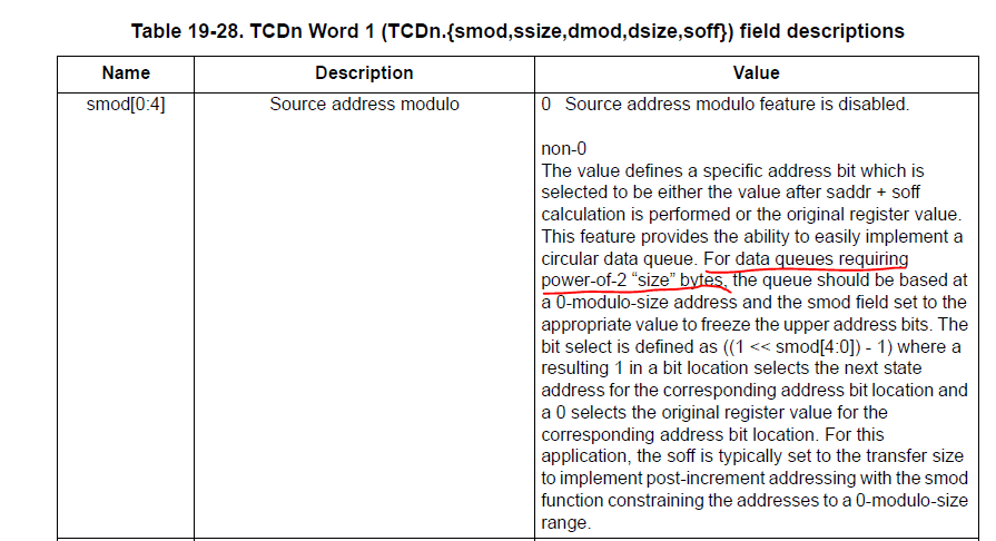
therefore ,the data queues requiring power-of-2 “size” bytes,is it right?
In AN4797 code example(attachment),
uint64_t forceOut_conf[] = {0x0000000080400800, 0x0008008080300800, 0x0000000080400800, 0x0000008080300800};
EDMA.CHANNEL[0].TCDWORD0_.B.SADDR = (uint32_t) (forceOut_conf); // Source address
EDMA.CHANNEL[0].TCDWORD4_.B.SMOD = 5; // Source address modulo
Because the forceOut_conf[] data queques totally have 32 size bytes, it needs change five address bits. So,the smod bit is 5,is it right?
Another question: what does "0-modulo-size" mean?
Thanks very much!
Yanna
- Mark as New
- Bookmark
- Subscribe
- Mute
- Subscribe to RSS Feed
- Permalink
- Report Inappropriate Content
Hi,
example 2 is correct. It's hexadecimal number, not binary...
Yes, data queues should be power-of-2 size.
Yes, smod=5 creates buffer size 32 bytes.
"0-modulo-size" - That's what I wrote in my last post: "If smod/dmod is used (different from 0) then saddr/daddr should be aligned accordingly. For example, if smod=3 then saddr should be aligned to 8 bytes."
Lukas
- Mark as New
- Bookmark
- Subscribe
- Mute
- Subscribe to RSS Feed
- Permalink
- Report Inappropriate Content
Hi,Lukas.
Sorry,I’m wrong. You are right. ‑_-
Thanks very much!
Yanna


