- Forums
- Product Forums
- General Purpose MicrocontrollersGeneral Purpose Microcontrollers
- i.MX Forumsi.MX Forums
- QorIQ Processing PlatformsQorIQ Processing Platforms
- Identification and SecurityIdentification and Security
- Power ManagementPower Management
- MCX Microcontrollers
- S32G
- S32K
- S32V
- MPC5xxx
- Other NXP Products
- Wireless Connectivity
- S12 / MagniV Microcontrollers
- Powertrain and Electrification Analog Drivers
- Sensors
- Vybrid Processors
- Digital Signal Controllers
- 8-bit Microcontrollers
- ColdFire/68K Microcontrollers and Processors
- PowerQUICC Processors
- OSBDM and TBDML
- S32M
-
- Solution Forums
- Software Forums
- MCUXpresso Software and ToolsMCUXpresso Software and Tools
- CodeWarriorCodeWarrior
- MQX Software SolutionsMQX Software Solutions
- Model-Based Design Toolbox (MBDT)Model-Based Design Toolbox (MBDT)
- FreeMASTER
- eIQ Machine Learning Software
- Embedded Software and Tools Clinic
- S32 SDK
- S32 Design Studio
- GUI Guider
- Zephyr Project
- Voice Technology
- Application Software Packs
- Secure Provisioning SDK (SPSDK)
- Processor Expert Software
- MCUXpresso Training Hub
-
- Topics
- Mobile Robotics - Drones and RoversMobile Robotics - Drones and Rovers
- NXP Training ContentNXP Training Content
- University ProgramsUniversity Programs
- Rapid IoT
- NXP Designs
- SafeAssure-Community
- OSS Security & Maintenance
- Using Our Community
-
- Cloud Lab Forums
-
- Knowledge Bases
- ARM Microcontrollers
- i.MX Processors
- Identification and Security
- Model-Based Design Toolbox (MBDT)
- QorIQ Processing Platforms
- S32 Automotive Processing Platform
- Wireless Connectivity
- CodeWarrior
- MCUXpresso Suite of Software and Tools
- MQX Software Solutions
-
Inquiries about setting up the MPC5777C Linker Directives (LD) file in the GHS development environme
Based on the sample code(MPC5777C-TSENS-Temp-calculation_v1.0-GHS614) provided on your website, I created a test code divided into two projects according to core0 or 1. also, referring to the LD file of the sample code, I edited the LD file according to the project as shown in the figure below so that the RAM and ROM areas of core0 and core1 can be separated.
-----------------------------------------------------------------------------------------------------------------------------------
Core 0 project LD file:
DEFAULTS {
SRAM_SIZE = 256K
SRAM_MMU_SIZE = 512K
SRAM_BASE_ADDR = 0x40000000
STACK_SIZE_0 = 4K // 4KB Stack for core 0
// STACK_SIZE_1 = 4k // 4KB Stack for core 1
stack_reserve = 4k
heap_reserve = 4k
}
MEMORY {
// 6M Internal Flash
flash_rsvd1 : ORIGIN = 0x00000000, LENGTH = 8
flash_memory1 : ORIGIN = ., LENGTH = 256K-8 // low-mid-high blocks
flash_rsvd2 : ORIGIN = 0x00800000, LENGTH = 8
flash_memory2 : ORIGIN = ., LENGTH = 8M-8 // large blocks
// 512KB of internal SRAM starting at 0x40000000
sram_rsvd1 : ORIGIN = 0x40000000, LENGTH = 0x200
sram_reset : ORIGIN = ., LENGTH = 0
sram_memory : ORIGIN = ., LENGTH = SRAM_SIZE-0x200
sram_rsvd2 : ORIGIN = ., LENGTH = 0
// 4k of stack per core to be locked in cache
stack_ram0 : ORIGIN = SRAM_BASE_ADDR+SRAM_MMU_SIZE, LENGTH = STACK_SIZE_0
// stack_ram1 : ORIGIN = SRAM_BASE_ADDR+SRAM_MMU_SIZE+STACK_SIZE_0, LENGTH = STACK_SIZE_1
}
-----------------------------------------------------------------------------------------------------------------------------------
Core 1 project LD file:
DEFAULTS {
SRAM_SIZE = 256K
SRAM_MMU_SIZE = 256K
SRAM_BASE_ADDR = 0x40040000
STACK_SIZE_0 = 4K // 4KB Stack for core 0
STACK_SIZE_1 = 4k // 4KB Stack for core 1
stack_reserve = 4k
heap_reserve = 4k
}
MEMORY {
// 6M Internal Flash
flash_rsvd1 : ORIGIN = 0x00000000, LENGTH = 8
flash_memory1 : ORIGIN = ., LENGTH = 256K-8 // low-mid-high blocks
flash_rsvd2 : ORIGIN = 0x00B00000, LENGTH = 8
flash_memory2 : ORIGIN = ., LENGTH = 5M-8 // large blocks
// 512KB of internal SRAM starting at 0x40040000
sram_rsvd1 : ORIGIN = 0x40040000, LENGTH = 0x200
sram_reset : ORIGIN = ., LENGTH = 0
sram_memory : ORIGIN = ., LENGTH = SRAM_SIZE-0x200
sram_rsvd2 : ORIGIN = ., LENGTH = 0
// 4k of stack per core to be locked in cache
// stack_ram0 : ORIGIN = SRAM_BASE_ADDR+SRAM_MMU_SIZE, LENGTH = STACK_SIZE_0
stack_ram1 : ORIGIN = SRAM_BASE_ADDR+SRAM_MMU_SIZE+STACK_SIZE_0, LENGTH = STACK_SIZE_1
}
-----------------------------------------------------------------------------------------------------------------------------------
After editing the LD file as above, if the code is loaded into the target and executed, Core 0 operates normally, but Core 1 normally executes the main function and enters the IVOR 6 interrupt.
My guess is that the RAM area allocation in the Core 1 LD file is set incorrectly, can you please tell me where I am wrong?(The start up code used sample code (__start))
Further debugging confirmed that Core1 does not copy interrupt vector table information from ROM to RAM.
In the init.s file (start coed) of the sample code you provided, core0 calls _start at the end of init.s, and core1 calls main(for the core1).
And, it is seems that Core0 copies the interrupt vector table from ROM to RAM at _start included in crt0.ppc.
I think that core1 needs a procedure to copy ROM data to RAM like core0, so I modified and executed init.s so that core1 calls _start included in crt0.ppc instead of main. However, core1 cannot enter main.
How can I make the provided sample code (integrated project of core0 and core1) into a separate project for each core? Any advice would be appreciated.
Hello,
Creating of multicore project need good understanding of the concept.
You can initialize both initialize everything from core0 (except core1 registers).
But if you want to separate it (usually done to speed up startup) then you need to have 2 dedicated startups. (one for each core)
First make sure your core0 boots correctly and starts core1.
Then find space in RAM where you want to initialize vectors. Copy table vector there in your startup. Don't forget about alignment of table in memory.
How can I make the provided sample code (integrated project of core0 and core1) into a separate project for each core? Any advice would be appreciated.
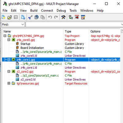
You simply create project with 2 outputs (elfs, or S-recors or any binary) and 2 linker files. This is the most simple way to handle multicore.
I do not have example code for MPC5777C, but here is how it looks like for 3 core device MPC5748G:
Best regards,
Peter
