- Forums
- Product Forums
- General Purpose MicrocontrollersGeneral Purpose Microcontrollers
- i.MX Forumsi.MX Forums
- QorIQ Processing PlatformsQorIQ Processing Platforms
- Identification and SecurityIdentification and Security
- Power ManagementPower Management
- Wireless ConnectivityWireless Connectivity
- RFID / NFCRFID / NFC
- MCX Microcontrollers
- S32G
- S32K
- S32V
- MPC5xxx
- Other NXP Products
- S12 / MagniV Microcontrollers
- Powertrain and Electrification Analog Drivers
- Sensors
- Vybrid Processors
- Digital Signal Controllers
- 8-bit Microcontrollers
- ColdFire/68K Microcontrollers and Processors
- PowerQUICC Processors
- OSBDM and TBDML
- S32M
-
- Solution Forums
- Software Forums
- MCUXpresso Software and ToolsMCUXpresso Software and Tools
- CodeWarriorCodeWarrior
- MQX Software SolutionsMQX Software Solutions
- Model-Based Design Toolbox (MBDT)Model-Based Design Toolbox (MBDT)
- FreeMASTER
- eIQ Machine Learning Software
- Embedded Software and Tools Clinic
- S32 SDK
- S32 Design Studio
- GUI Guider
- Zephyr Project
- Voice Technology
- Application Software Packs
- Secure Provisioning SDK (SPSDK)
- Processor Expert Software
-
- Topics
- Mobile Robotics - Drones and RoversMobile Robotics - Drones and Rovers
- NXP Training ContentNXP Training Content
- University ProgramsUniversity Programs
- Rapid IoT
- NXP Designs
- SafeAssure-Community
- OSS Security & Maintenance
- Using Our Community
-
- Cloud Lab Forums
-
- Knowledge Bases
- ARM Microcontrollers
- i.MX Processors
- Identification and Security
- Model-Based Design Toolbox (MBDT)
- QorIQ Processing Platforms
- S32 Automotive Processing Platform
- Wireless Connectivity
- CodeWarrior
- MCUXpresso Suite of Software and Tools
- MQX Software Solutions
-
- Home
- :
- QorIQ处理平台
- :
- Layerscape
- :
- DDR Mapping Registers for ls1043a
DDR Mapping Registers for ls1043a
DDR Mapping Registers for ls1043a
Hi,
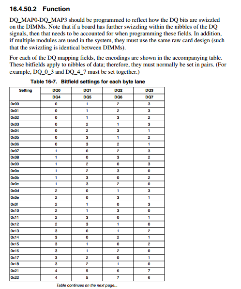
I am trying to configure the DDR Memory Controller's registers of ls1043a.I am unable to comprehend the "DQ mapping registers." Can anybody explain what they are for and how to configure them for support ecc.
Please refer to the JEDEC Standard No. 21-C
Annex L: Serial Presence Detect (SPD) for DDR4 SDRAM Modules:
“Bytes 60~77 (0x03C~0x04D): Connector to SDRAM Bit Mapping
These bytes document the connection between data signals at the edge connector of a module to the DDR4 SDRAM inputs pins for package rank 0 of the module. This information is used by the controller to route data onto the correct bit lines for CRC transmission as described in the DDR4 SDRAM data sheet JESD79-4. Each byte describes the mapping for one nibble (four bits) of data. In addition, each SPD byte describes the mapping between package rank 0 bits and equivalent bits in other ranks.”
The CRC generation and checking is described in the JEDEC Standard No. 79-4, 4.16 CRC
