- Forums
- Product Forums
- General Purpose MicrocontrollersGeneral Purpose Microcontrollers
- i.MX Forumsi.MX Forums
- QorIQ Processing PlatformsQorIQ Processing Platforms
- Identification and SecurityIdentification and Security
- Power ManagementPower Management
- Wireless ConnectivityWireless Connectivity
- RFID / NFCRFID / NFC
- MCX Microcontrollers
- S32G
- S32K
- S32V
- MPC5xxx
- Other NXP Products
- S12 / MagniV Microcontrollers
- Powertrain and Electrification Analog Drivers
- Sensors
- Vybrid Processors
- Digital Signal Controllers
- 8-bit Microcontrollers
- ColdFire/68K Microcontrollers and Processors
- PowerQUICC Processors
- OSBDM and TBDML
- S32M
-
- Solution Forums
- Software Forums
- MCUXpresso Software and ToolsMCUXpresso Software and Tools
- CodeWarriorCodeWarrior
- MQX Software SolutionsMQX Software Solutions
- Model-Based Design Toolbox (MBDT)Model-Based Design Toolbox (MBDT)
- FreeMASTER
- eIQ Machine Learning Software
- Embedded Software and Tools Clinic
- S32 SDK
- S32 Design Studio
- GUI Guider
- Zephyr Project
- Voice Technology
- Application Software Packs
- Secure Provisioning SDK (SPSDK)
- Processor Expert Software
-
- Topics
- Mobile Robotics - Drones and RoversMobile Robotics - Drones and Rovers
- NXP Training ContentNXP Training Content
- University ProgramsUniversity Programs
- Rapid IoT
- NXP Designs
- SafeAssure-Community
- OSS Security & Maintenance
- Using Our Community
-
- Cloud Lab Forums
-
- Knowledge Bases
- ARM Microcontrollers
- i.MX Processors
- Identification and Security
- Model-Based Design Toolbox (MBDT)
- QorIQ Processing Platforms
- S32 Automotive Processing Platform
- Wireless Connectivity
- CodeWarrior
- MCUXpresso Suite of Software and Tools
- MQX Software Solutions
-
Hello,
We are designing the implantable device using LPC55S1 MCU and want to bypass the internal DCDC converter to avoid using an inductor.
I have read this post on the forum and understood the requirement and the unused pin connection.
Still need to figure out what will be the proper power up sequence to supply the core voltage to MCU.
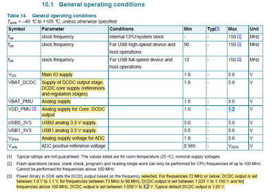
Both USB0 and USB1 are used and the VBAT = 1.8V in our design, hence we do have 3 distinct voltage rails: 1.8V(VBAT), 3.3V(USB), 1.1V(Core)
Could you please guide the proper powering up sequence in such case?
One additional question regarding using 1.2V for the core (I know it has already been discussed in the previous post) is that what would be the trade-off using 1.2V for all frequency range ( less than 100MHz), assuming that the supply is well controlled not to exceed the maximum rating of VDD_PMU (1.26Vmax_absolute)?
Best,
Jaehoon
已解决! 转到解答。
Hi,
As you know that the LDO can provide stable output supply voltage with low efficiency, while the DC/DC converter can provide output supply voltage with ripple but high efficiency.
Regarding the recommendation of internal DC/Dc converter, based on AE team advise, we never fully tested for using external LDO for the VDD_PMU power supply.
But I think it is okay, you can use 1.2V LDO for the VDD_PMU, which will cover all the core clock frequency.
Hope it can help you
BR
Xiangjun Rong
Hi,
I suppose that you have power supply rails:
1.8V for for VDD, VDDA,Vrefp, VBAT_DCDC, VBAT_PMU pins
3.3V for USB0_3V3, USB1_3V3 pins
1.1V for VDD_PMU
The 1.8V starts-up firstly, the 1.1V appears secondly. The USBx_3v3 pins provide power for only USB module, they can appear anytime.
Anyway, we suggest you use internal DC/Dc converter.
Hope it can help you
BR
XiangJun Rong
Thanks XiangJun for your reply.
Could you please explain more details of the potential risks of not using an internal DCDC?
Is it purely because of setting a different voltage level depending on the operating frequency? What is the downside of using a higher voltage (such as 1.2V) for all frequency range? Maybe more power consumption?
I would like to understand the trade-offs between using an internal DCDC versus external LDO.
Best,
Jaehoon
Hi,
As you know that the LDO can provide stable output supply voltage with low efficiency, while the DC/DC converter can provide output supply voltage with ripple but high efficiency.
Regarding the recommendation of internal DC/Dc converter, based on AE team advise, we never fully tested for using external LDO for the VDD_PMU power supply.
But I think it is okay, you can use 1.2V LDO for the VDD_PMU, which will cover all the core clock frequency.
Hope it can help you
BR
Xiangjun Rong
