- Forums
- Product Forums
- General Purpose MicrocontrollersGeneral Purpose Microcontrollers
- i.MX Forumsi.MX Forums
- QorIQ Processing PlatformsQorIQ Processing Platforms
- Identification and SecurityIdentification and Security
- Power ManagementPower Management
- MCX Microcontrollers
- S32G
- S32K
- S32V
- MPC5xxx
- Other NXP Products
- Wireless Connectivity
- S12 / MagniV Microcontrollers
- Powertrain and Electrification Analog Drivers
- Sensors
- Vybrid Processors
- Digital Signal Controllers
- 8-bit Microcontrollers
- ColdFire/68K Microcontrollers and Processors
- PowerQUICC Processors
- OSBDM and TBDML
- S32M
-
- Solution Forums
- Software Forums
- MCUXpresso Software and ToolsMCUXpresso Software and Tools
- CodeWarriorCodeWarrior
- MQX Software SolutionsMQX Software Solutions
- Model-Based Design Toolbox (MBDT)Model-Based Design Toolbox (MBDT)
- FreeMASTER
- eIQ Machine Learning Software
- Embedded Software and Tools Clinic
- S32 SDK
- S32 Design Studio
- GUI Guider
- Zephyr Project
- Voice Technology
- Application Software Packs
- Secure Provisioning SDK (SPSDK)
- Processor Expert Software
- MCUXpresso Training Hub
-
- Topics
- Mobile Robotics - Drones and RoversMobile Robotics - Drones and Rovers
- NXP Training ContentNXP Training Content
- University ProgramsUniversity Programs
- Rapid IoT
- NXP Designs
- SafeAssure-Community
- OSS Security & Maintenance
- Using Our Community
-
- Cloud Lab Forums
-
- Knowledge Bases
- ARM Microcontrollers
- i.MX Processors
- Identification and Security
- Model-Based Design Toolbox (MBDT)
- QorIQ Processing Platforms
- S32 Automotive Processing Platform
- Wireless Connectivity
- CodeWarrior
- MCUXpresso Suite of Software and Tools
- MQX Software Solutions
-
- Home
- :
- 汎用マイクロコントローラ
- :
- LPCマイクロコントローラ
- :
- LPC55S69 Debug Problem with JLink V9
LPC55S69 Debug Problem with JLink V9
- RSS フィードを購読する
- トピックを新着としてマーク
- トピックを既読としてマーク
- このトピックを現在のユーザーにフロートします
- ブックマーク
- 購読
- ミュート
- 印刷用ページ
LPC55S69 Debug Problem with JLink V9
- 新着としてマーク
- ブックマーク
- 購読
- ミュート
- RSS フィードを購読する
- ハイライト
- 印刷
- 不適切なコンテンツを報告
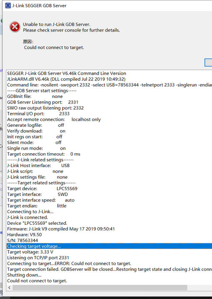
Recently i have made an LPC55S69 basic-system PCB equiped with a standard SWD(SWCLK,SWDIO,SWO and RESET signal) Debug probe.But when i conneted my jlink to the board and pressed debug button in mcuxpresso ide with an opened example GPIO project import from the SDK,errors showed "connot connect to the tartget".However,the debugger has detected the mcu's Model.
I have checked my PCB routes and SCH connections,it seems I have made everthing properly, 10K pull-up resistor on SWCLK and SWDIO or default jtag pin connections.
Did anybody ever make a circuit board based on this mcu?Could anyone tell me the debug result about his own board?
- 新着としてマーク
- ブックマーク
- 購読
- ミュート
- RSS フィードを購読する
- ハイライト
- 印刷
- 不適切なコンテンツを報告
Hi WM
Please refer this article to design your debug interface
Design Considerations for Debug
Have a nice day
Jun Zhang
-------------------------------------------------------------------------------
Note:
- If this post answers your question, please click the "Mark Correct" button. Thank you!
- We are following threads for 7 weeks after the last post, later replies are ignored
Please open a new thread and refer to the closed one, if you have a related question at a later point in time.
-------------------------------------------------------------------------------
