- Forums
- Product Forums
- General Purpose MicrocontrollersGeneral Purpose Microcontrollers
- i.MX Forumsi.MX Forums
- QorIQ Processing PlatformsQorIQ Processing Platforms
- Identification and SecurityIdentification and Security
- Power ManagementPower Management
- Wireless ConnectivityWireless Connectivity
- RFID / NFCRFID / NFC
- Advanced AnalogAdvanced Analog
- MCX Microcontrollers
- S32G
- S32K
- S32V
- MPC5xxx
- Other NXP Products
- S12 / MagniV Microcontrollers
- Powertrain and Electrification Analog Drivers
- Sensors
- Vybrid Processors
- Digital Signal Controllers
- 8-bit Microcontrollers
- ColdFire/68K Microcontrollers and Processors
- PowerQUICC Processors
- OSBDM and TBDML
- S32M
- S32Z/E
-
- Solution Forums
- Software Forums
- MCUXpresso Software and ToolsMCUXpresso Software and Tools
- CodeWarriorCodeWarrior
- MQX Software SolutionsMQX Software Solutions
- Model-Based Design Toolbox (MBDT)Model-Based Design Toolbox (MBDT)
- FreeMASTER
- eIQ Machine Learning Software
- Embedded Software and Tools Clinic
- S32 SDK
- S32 Design Studio
- GUI Guider
- Zephyr Project
- Voice Technology
- Application Software Packs
- Secure Provisioning SDK (SPSDK)
- Processor Expert Software
- Generative AI & LLMs
-
- Topics
- Mobile Robotics - Drones and RoversMobile Robotics - Drones and Rovers
- NXP Training ContentNXP Training Content
- University ProgramsUniversity Programs
- Rapid IoT
- NXP Designs
- SafeAssure-Community
- OSS Security & Maintenance
- Using Our Community
-
- Cloud Lab Forums
-
- Knowledge Bases
- ARM Microcontrollers
- i.MX Processors
- Identification and Security
- Model-Based Design Toolbox (MBDT)
- QorIQ Processing Platforms
- S32 Automotive Processing Platform
- Wireless Connectivity
- CodeWarrior
- MCUXpresso Suite of Software and Tools
- MQX Software Solutions
- RFID / NFC
- Advanced Analog
-
- NXP Tech Blogs
- Home
- :
- 汎用マイクロコントローラ
- :
- LPCマイクロコントローラ
- :
- Re: LPC54114 DMA Linked Transfer Ping Pong - Circular Buffers
LPC54114 DMA Linked Transfer Ping Pong - Circular Buffers
- RSS フィードを購読する
- トピックを新着としてマーク
- トピックを既読としてマーク
- このトピックを現在のユーザーにフロートします
- ブックマーク
- 購読
- ミュート
- 印刷用ページ
LPC54114 DMA Linked Transfer Ping Pong - Circular Buffers
- 新着としてマーク
- ブックマーク
- 購読
- ミュート
- RSS フィードを購読する
- ハイライト
- 印刷
- 不適切なコンテンツを報告
Hello:
Introduction:
I am having a difficult problem with the DMA engine in the LPC54114. I am trying to use the DMA in a continuously linked transfer described on page 160 of User Manual 1.4 UM10914. Instead of a ping pong, I am setting up 4 descriptors where the last one links back to the 1st. I am transferring data from the ADC into some memory buffers. To test, I am feeding the ADC with a known frequency sine wave.
Observed Issue:
The 1st four transfers always work OK. If I terminate the transfer at the 4th descriptor, I can looked at the data and it is correct. If I link the 4th descriptor back to the 1st, data in my memory buffer is incorrect after the 1st four transfers. It looks like it is ADC data BUT it is out of order. I cannot find a pattern to the out of order data but it only appears to occur after the 1st set of 4 descriptors are executed.
Also note, that the DMA is continually operating. It is doing the correct number if transfers, it just is not moving to the correct destination addresses. It does appear the DMA is moving data into the correct region, but the actual ordering is messed up. I am monitoring via a pin on an o-scope when I get a DMA IRQ as well as when the ADC is triggered via the SCT. I get ADC & DMA pulses at the correct rate, etc.
Background:
Here is a description of of the DMA setup.
/*
* We need a total of 5 Descriptors
*
* 1 Descriptor that is in the main SRAM table to start
*
* 4 to maintain the continuous transfer. (See Page 160 of User Manual 1.4 UM10914)
*
* There will always be 1 buffer getting new data while the other 3 are being processed.
*
*
*/
/* DMA descriptor for memory to memory operation - note that addresses must
* be the END address for src and destination, not the starting address.
* DMA operations moves from end to start.
*
*/
     /*
     *
     *         +------------+
     *        |   Initial  |       Next
     *        |            +------------+
     *        | Descriptor |            |
     *        +------------+            |
     *                                  |
     *        +------------+      +-----v------+      +------------+      +------------+
     *        |    ADC     | Next |    ADC     | Next |    ADC     | Next |    ADC     | Next
     *  +-----> Descriptor +------> Descriptor +------> Descriptor +------> Descriptor +-----+
     *  |     |     0      |      |     1      |      |     2      |      |     3      |     |
     *  |     +------------+      +------------+      +------------+      +------------+     |
     *  |                                                                                    |
     *  |                                                                                    |
     *  +------------------------------------------------------------------------------------+
     *
*/I am using the setup to get a set of 4 buffers such that I can have 4 at any time to process
/*
In the figure below, B0,B1 and B2 form a complete buffer that
needs to be processed. Since we are doing overlaps of 3,
we can wrap the pointer to the data exactly when we need to.
Buffer State 0 1 2 3
+----------+ +----------+ +----------+ +----------+
| | | | | | | |
| Just | | | | | | Next To |
| Filled | | | | | | Fill |
| B2 | | B1 | | B0 | | |
+----------+ +----------+ +----------+ +----------+
| | | | | | | |
| Next To | | Just | | | | |
| Fill | | Filled | | | | |
| | | B2 | | B1 | | B0 |
+----------+ +----------+ +----------+ +----------+
| | | | | | | |
| | | Next To | | Just | | |
| | | Fill | | Filled | | |
| B0 | | | | B2 | | B1 |
+----------+ +----------+ +----------+ +----------+
| | | | | | | |
| | | | | Next To | | Just |
| | | | | Fill | | Filled |
| B1 | | B0 | | | | B2 |
+----------+ +----------+ +----------+ +----------+
*/Here is the Setup routine:
#define NUM_BUFFERS 4
#define DMA_TRANSFER_SIZE 8
__BSS(RAM2) ALIGN(512) DMA_CHDESC_T ADC_TransferDescriptors[4];
uint16_t CapturedData[NUM_BUFFERS * DMA_TRANSFER_SIZE];
void InitADC()
{
DMA_CHDESC_T Initial_DMA_Descriptor;
/***
* ____ _
* / ___| __ _ _ __ ___ _ __ | | ___
* \___ \ / _` | '_ ` _ \| '_ \| |/ _ \
* ___) | (_| | | | | | | |_) | | __/
* |____/ \__,_|_| |_| |_| .__/|_|\___|
* | _ \ __ _| |_ ___ |_|
* | |_) / _` | __/ _ \
* | _ < (_| | || __/
* |_|_\_\__,_|\__\___|
* / ___| ___| |_ _ _ _ __
* \___ \ / _ \ __| | | | '_ \
* ___) | __/ |_| |_| | |_) |
* |____/ \___|\__|\__,_| .__/
* |_|
*/
/*
*
* Configure SCT0 channel 7. This is hardwired in the LPC54114 to
* trigger the ADC
*
*/
/* Initialize the SCT as PWM and set frequency */
Chip_SCTPWM_Init(LPC_SCT);
/* Stop the SCT before configuration */
Chip_SCTPWM_Stop(LPC_SCT);
/* Set MATCH0 for max limit */
LPC_SCT->REGMODE_L = 0;
LPC_SCT->REGMODE_H = 0;
Chip_SCT_SetMatchCount(LPC_SCT, SCT_MATCH_0, 0);
//At the high frequencies, we have rough control over frequency
//Starting with a 640Khz Fs
//A value of 150 maps evenly to 640Khz. (96MHz/150)
Chip_SCT_SetMatchReload(LPC_SCT, SCT_MATCH_0, 960);
LPC_SCT->EVENT[0].CTRL = 1 << 12;
LPC_SCT->EVENT[0].STATE = 1;
/* Set SCT Counter to count 32-bits and reset to 0 after reaching MATCH0 */
Chip_SCT_Config(LPC_SCT, SCT_CONFIG_32BIT_COUNTER | SCT_CONFIG_AUTOLIMIT_L);
/* Use SCT0_OUT7 pin to monitor the ADC trigger signal*/
Chip_IOCON_PinMuxSet(LPC_IOCON, 1, 14, IOCON_FUNC3 | IOCON_MODE_INACT | IOCON_DIGITAL_EN | IOCON_INPFILT_OFF);
Chip_SCTPWM_SetOutPin(LPC_SCT, SCT_PWM_OUT, SCT_PWM_PIN_OUT);
//Use 1tick of, the other ticks off for a nice pulse
Chip_SCTPWM_SetDutyCycle(LPC_SCT, SCT_PWM_OUT, 1);
Chip_SCTPWM_Start(LPC_SCT);
/***
* ____ __ __ _
* | _ \| \/ | / \
* | | | | |\/| | / _ \
* | |_| | | | |/ ___ \
* |____/|_| |_/_/ \_\
* / ___| ___| |_ _ _ _ __
* \___ \ / _ \ __| | | | '_ \
* ___) | __/ |_| |_| | |_) |
* |____/ \___|\__|\__,_| .__/
* |_|
*/
/*
* We need a total of 5 Descriptors
*
* 1 Descriptor that is in the main SRAM table to start
*
* 4 to maintain the continuous transfer. (See Page 160 of User Manual 1.4 UM10914)
*
* There will always be 1 buffer getting new data while the other 3 are being processed.
*
*
*/
/* DMA descriptor for memory to memory operation - note that addresses must
* be the END address for src and destination, not the starting address.
* DMA operations moves from end to start.
*
*/
/*
*
* +------------+
* | Initial | Next
* | +------------+
* | Descriptor | |
* +------------+ |
* |
* +------------+ +-----v------+ +------------+ +------------+
* | ADC | Next | ADC | Next | ADC | Next | ADC | Next
* +-----> Descriptor +------> Descriptor +------> Descriptor +------> Descriptor +-----+
* | | 0 | | 1 | | 2 | | 3 | |
* | +------------+ +------------+ +------------+ +------------+ |
* | |
* | |
* +------------------------------------------------------------------------------------+
*
*/
ADC_TransferDescriptors[0].source = (uint32_t)&LPC_ADC->DAT[1];
ADC_TransferDescriptors[1].source = (uint32_t)&LPC_ADC->DAT[1];
ADC_TransferDescriptors[2].source = (uint32_t)&LPC_ADC->DAT[1];
ADC_TransferDescriptors[3].source = (uint32_t)&LPC_ADC->DAT[1];
ADC_TransferDescriptors[0].dest = (uint32_t)&CapturedData[(0+1)*DMA_TRANSFER_SIZE-1];
ADC_TransferDescriptors[1].dest = (uint32_t)&CapturedData[(1+1)*DMA_TRANSFER_SIZE-1];
ADC_TransferDescriptors[2].dest = (uint32_t)&CapturedData[(2+1)*DMA_TRANSFER_SIZE-1];
ADC_TransferDescriptors[3].dest = (uint32_t)&CapturedData[(3+1)*DMA_TRANSFER_SIZE-1];
//The initial DMA desciptor is the same as the 1st transfer descriptor. It
//Will link into the 2nd of the main descriptors.
ADC_TransferDescriptors[0].next = (uint32_t)&ADC_TransferDescriptors[1];
ADC_TransferDescriptors[1].next = (uint32_t)&ADC_TransferDescriptors[2];
ADC_TransferDescriptors[2].next = (uint32_t)&ADC_TransferDescriptors[3];
ADC_TransferDescriptors[3].next = (uint32_t)&ADC_TransferDescriptors[0];
ADC_TransferDescriptors[0].xfercfg = (DMA_XFERCFG_CFGVALID |
DMA_XFERCFG_RELOAD |
DMA_XFERCFG_SETINTA |
DMA_XFERCFG_WIDTH_16 |
DMA_XFERCFG_SRCINC_0 |
DMA_XFERCFG_DSTINC_1 |
DMA_XFERCFG_XFERCOUNT(DMA_TRANSFER_SIZE));
ADC_TransferDescriptors[1].xfercfg = ADC_TransferDescriptors[0].xfercfg;
ADC_TransferDescriptors[2].xfercfg = ADC_TransferDescriptors[0].xfercfg;
ADC_TransferDescriptors[3].xfercfg = (DMA_XFERCFG_CFGVALID |
DMA_XFERCFG_RELOAD |
DMA_XFERCFG_SETINTA |
DMA_XFERCFG_WIDTH_16 |
DMA_XFERCFG_SRCINC_0 |
DMA_XFERCFG_DSTINC_1 |
DMA_XFERCFG_XFERCOUNT(DMA_TRANSFER_SIZE));
Initial_DMA_Descriptor.source = ADC_TransferDescriptors[0].source;
Initial_DMA_Descriptor.dest = ADC_TransferDescriptors[0].dest;
Initial_DMA_Descriptor.next = (uint32_t)&ADC_TransferDescriptors[1];
Initial_DMA_Descriptor.xfercfg = ADC_TransferDescriptors[0].xfercfg;
/* DMA initialization - enable DMA clocking and reset DMA if needed */
Chip_DMA_Init(LPC_DMA);
/* Enable DMA controller and use driver provided DMA table for current descriptors */
Chip_DMA_Enable(LPC_DMA);
Chip_DMA_SetSRAMBase(LPC_DMA, DMA_ADDR(Chip_DMA_Table));
/* Setup channel 0 for the following configuration:
- High channel priority
- Interrupt A fires on descriptor completion */
Chip_DMA_EnableChannel(LPC_DMA, DMA_CH0);
Chip_DMA_EnableIntChannel(LPC_DMA, DMA_CH0);
Chip_DMA_SetupChannelConfig(LPC_DMA, DMA_CH0,
//(DMA_CFG_PERIPHREQEN |
(DMA_CFG_HWTRIGEN |
DMA_CFG_TRIGBURST_BURST |
DMA_CFG_TRIGTYPE_EDGE |
DMA_CFG_TRIGPOL_HIGH |
DMA_CFG_BURSTPOWER_1 |
DMA_CFG_CHPRIORITY(0)
)
);
//make sure ADC Sequence A interrupts is selected for for a DMA trigger
LPC_INMUX->DMA_ITRIG_INMUX[0] = 0;
/* Enable DMA interrupt */
NVIC_EnableIRQ(DMA_IRQn);
// The 1st descriptor is set up through the registers.
/* Setup transfer descriptor and validate it */
Chip_DMA_SetupTranChannel(LPC_DMA, DMA_CH0, &Initial_DMA_Descriptor);
//Use the transfer configuration for our 4 main descriptors
Chip_DMA_SetupChannelTransfer(LPC_DMA, DMA_CH0,
ADC_TransferDescriptors[0].xfercfg
);
Chip_DMA_SetValidChannel(LPC_DMA, DMA_CH0);
/***
* _ ____ ____
* / \ | _ \ / ___|
* / _ \ | | | | |
* / ___ \| |_| | |___
* /_/__ \_\____/ \____|
* / ___| ___| |_ _ _ _ __
* \___ \ / _ \ __| | | | '_ \
* ___) | __/ |_| |_| | |_) |
* |____/ \___|\__|\__,_| .__/
* |_|
*/
ADC_BufferState = 0;
/* Initialization ADC to 12 bit and set clock divide to 2 to operate synchronously at System clock/2 */
Chip_ADC_Init(LPC_ADC, ADC_CR_RESOL(3) | ADC_CR_CLKDIV(0));
//select ADC Channel 1 as input
Chip_IOCON_PinMuxSet(LPC_IOCON, 0, 30, IOCON_FUNC0 | IOCON_ANALOG_EN| IOCON_INPFILT_OFF);
/* Enable Channel 1 conversion in Sequence A */
LPC_ADC->INSEL = 0x01;
Chip_ADC_SetupSequencer(LPC_ADC,
ADC_SEQA_IDX,
ADC_SEQ_CTRL_SEQ_ENA |
ADC_SEQ_CTRL_CHANNEL_EN(ADC_INPUT_CHANNEL) |
ADC_SEQ_CTRL_TRIGGER(2) |
ADC_SEQ_CTRL_HWTRIG_POLPOS |
ADC_SEQ_CTRL_MODE_EOS);
/* Enable Sequence A interrupt */
Chip_ADC_EnableInt(LPC_ADC, ADC_INTEN_SEQA_ENABLE);
/* Calibrate ADC */
if(Chip_ADC_Calibration(LPC_ADC) == LPC_OK)
{
/* Enable ADC SeqA Interrupt */
// NVIC_EnableIRQ(ADC_SEQA_IRQn);
/* Enable SysTick Timer */
//SysTick_Config(SystemCoreClock / 100);
}
else {
DEBUGSTR("ADC Calibration Failed \r\n");
Board_LED_Set(0, true);
return 0;
}
}
The DMA handler:
void DMA_IRQHandler(void)
{
Chip_GPIO_SetPinState(LPC_GPIO,TEST_PORT,true);
/* Rrror interrupt on channel 0? */
if ((Chip_DMA_GetIntStatus(LPC_DMA) & DMA_INTSTAT_ACTIVEERRINT) != 0)
{
/* This shouldn't happen for this simple DMA example, so set the LED
to indicate an error occurred. This is the correct method to clear
an abort. */
Chip_DMA_DisableChannel(LPC_DMA, DMA_CH0);
while ((Chip_DMA_GetBusyChannels(LPC_DMA) & (1 << DMA_CH0)) != 0) {}
Chip_DMA_AbortChannel(LPC_DMA, DMA_CH0);
Chip_DMA_ClearErrorIntChannel(LPC_DMA, DMA_CH0);
Chip_DMA_EnableChannel(LPC_DMA, DMA_CH0);
Board_LED_Set(0, true);
}
ADC_BufferState++;
ADC_BufferState &= 0x03;
/* Clear DMA interrupt for the channel */
LPC_DMA->DMACOMMON[0].INTA = 1;
}
I can upload my entire source code if needed. The only other pieces I have not shown is the main routine which calls the InitADC() function.
I will certainly post the results if I solve the issue. Hopefully someone else has seen this behavior.
- 新着としてマーク
- ブックマーク
- 購読
- ミュート
- RSS フィードを購読する
- ハイライト
- 印刷
- 不適切なコンテンツを報告
Hi Dingelen,
Many thanks and I haven't got involved in LPC5500-series support, William Jiang can assign resource.
By the way, after q quick review of this thread, the conclusion
- "If I didn't increment the destination of an descriptor when it is completed (i.e., next reload of this descriptor will overwrite the previous data), then the next time, this descriptor will get corrupted data"
shows an unreasonable design of LPC54-series DMA, and it could have been solved in LPC5500-series.
- 新着としてマーク
- ブックマーク
- 購読
- ミュート
- RSS フィードを購読する
- ハイライト
- 印刷
- 不適切なコンテンツを報告
Super example. Much better than the ones in the SDK... Thanks!
Is there a same example available for the LPC55-series? There seem to be some differences in how to set-up the DMA compared to the LPC54 series.
- 新着としてマーク
- ブックマーク
- 購読
- ミュート
- RSS フィードを購読する
- ハイライト
- 印刷
- 不適切なコンテンツを報告
Thanks for checking in on this thread and thanks to Rocky for helping verify the issue.
It was not possible to get my use case working on this chip. The descriptors would get corrupted. I was trying to get a continuous stream of data sampled into a set of of 4 buffers (the number actually didn't matter). The fix ended up requiring too much CPU time as the DMA would corrupt the descriptors. In my case the descriptors never would change all that much as they would point to the same blocks of memory.
I have not used the DMA on the LPC55 but I would certainly test to see if it is fixed.
- 新着としてマーク
- ブックマーク
- 購読
- ミュート
- RSS フィードを購読する
- ハイライト
- 印刷
- 不適切なコンテンツを報告
Hi Eli,
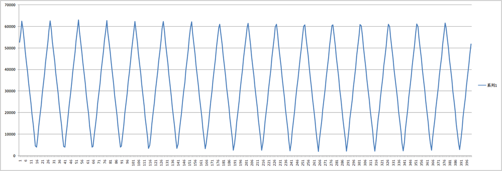
I used your method to export to excel, with my setup: 2 descriptors each transfer size is 4, 256 rollbacks(I re-configure destination in DMA ISR to make descriptor to increment to fill later buffer addresses, except for last rollback), I got almost perfect sampled data with waveform for more than 2000 samples, below is the waveform for first 400 samples (50 rollbacks):
I use triangle waveform to fill the ADC pin.
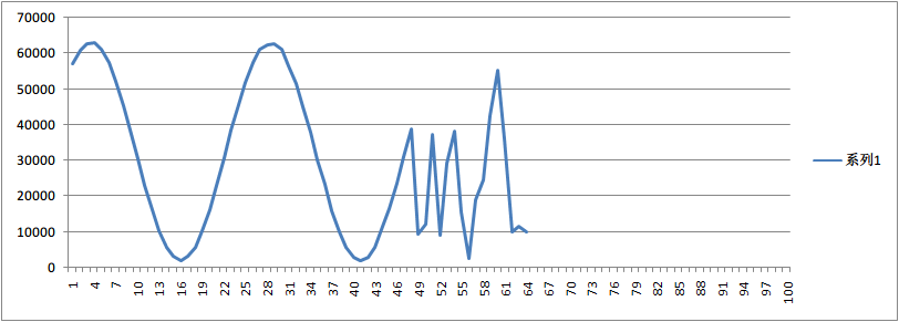
With your code indeed the data is corrupted, and later I found with my code the last iteration has corrupted data, now it seems to me if I didn't increment the destination of an descriptor when it is completed (i.e., next reload of this descriptor will overwrite the previous data), then the next time, this descriptor will get corrupted data.
Below graph has 3 iterations, the last iteration does not increment the descriptor target address so new data always overwrite old data in the next interation (rollback), and is corrupted.
If you set "DMA_LOOP_CNT" macro of my code to 1 then it is exactly like what happend in your code.
- 新着としてマーク
- ブックマーク
- 購読
- ミュート
- RSS フィードを購読する
- ハイライト
- 印刷
- 不適切なコンテンツを報告
Today I took several hours to try to reproduce your issue, but I didn't reproduce.
In the attached code (You just replace with your M4.c), I set
#define NUM_BUFFERS 2
#define DMA_TRANSFER_SIZE 4
#define DMA_LOOP_CNT 256
I modified the code to make the descriptors fill larger range of memory: After the descriptor is completed, in DMA IRQ, I update its target address to increment by "NUM_BUFFERS * DMA_TRANSFER_SIZE * sizeof(CapturedData[0])", and I define "DMA_LOOP_CNT" macro to specify how many loops of the linked descriptors.
I also set system clock to 48MHz by "Chip_Clock_SetSysClockDiv(2);", ADC trigger rate 48M/192= 250kHz.
By this way I collected 255 rounds of data, I didn't see data loss when DMA roll back to first descriptor,
I use triangle waveform to make it more linear so easy to observe.
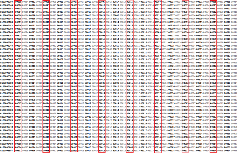
Below is the differential values (I showed more than 1000 samples, that is more than 128 rollbacks) of the samples, divided by 64, i.e., abs(sample[x] - sample[x-1]) / 64, for better observation, I didn’t know how you exported the data to excel, so I just take a screen shot and mark.
I use red blocks to highlight the first word of a descriptor, I didn't see abnormal large differential values in red blocks.
- 新着としてマーク
- ブックマーク
- 購読
- ミュート
- RSS フィードを購読する
- ハイライト
- 印刷
- 不適切なコンテンツを報告
Rocky: I was able to replicate your result. I did notice one large difference between your version and mine. Your code constantly moves the destination of the DMA. I remove the code that did the differenceing and applied a sine wave. The since wave looked correct except fo rthe last block. Also, the DMA transfer in your code eventually stops. If set it up to reuse memory (link in my previous examples) it no longer works.
Another important note:
Going back to my original program.... I did find an interesting combination that did work with the loopback on the descriptors that required 2 simple changes.
1.) Configure the DMA channel to start on the *NEGATIVE* edge of the trigger
Chip_DMA_SetupChannelConfig(LPC_DMA, DMA_CH0,
//(DMA_CFG_PERIPHREQEN |
(DMA_CFG_HWTRIGEN |
DMA_CFG_TRIGBURST_BURST |
DMA_CFG_TRIGTYPE_EDGE |
DMA_CFG_TRIGPOL_LOW |
DMA_CFG_BURSTPOWER_1 |
DMA_CFG_CHPRIORITY(0)
)
);2.) Enable Interrupts in the NVIC for ADC sequence A and clear all the flags.
void ADC_SEQA_IRQHandler(void)
{
Chip_ADC_ClearFlags(LPC_ADC,0xFFFFFFFF);
}If I make these changes, the DMA data looks correct and I can use a set of 4 continuously linked descriptors. This is a problem for general usage as the IRQ on ever sample uses quite a bit of CPU time.
Also, I still think there is some sort of synchronization problem in the chip. #2 should not be required as the manual states that the DMA controller takes care of this. If I don't clear the flags in the ADC IRQ routine, the DMA IRQ never fires.
- 新着としてマーク
- ブックマーク
- 購読
- ミュート
- RSS フィードを購読する
- ハイライト
- 印刷
- 不適切なコンテンツを報告
Hi Eli,
If I set the trigger edge to “DMA_CFG_TRIGPOL_LOW” then I can’t trigger DMA.
The one thing I observed is: In the linked ring descriptor usage, If a descriptor is reloaded by DMA w/o its destination address get updated, then ADC data sampled by this descriptor, which overwrites the old data, is corrupted.
However, if a descriptor’s data is overwritten by other descriptor(s), then data looks fine.
So in practice, user need to avoid data get overwritten by DMA, I think this shall be almost (if not all) the use case.
Best regards,
Rocky Song (宋岩)
Tel: 86-21-22052810
- 新着としてマーク
- ブックマーク
- 購読
- ミュート
- RSS フィードを購読する
- ハイライト
- 印刷
- 不適切なコンテンツを報告
Thank you for taking the time to do this on the hardware. If you tried my code without modification, did you see the same issue as I did?
I will run your version this weekend to try to figure things out.
1.) To get data in excel: I added the variable to the expressions window to get a list of values in the array. I then just copy and pasted the grid of data into excel.
2.) I did try lowering system clock as your code does but it had no effect. Chip_Clock_SetSysClockDiv(2);
3.) I will also try to get a hold of another board and/or chip.
- 新着としてマーク
- ブックマーク
- 購読
- ミュート
- RSS フィードを購読する
- ハイライト
- 印刷
- 不適切なコンテンツを報告
Hi Eli,
I remembered you once found 22nd sample get lost when descriptors' transfer size is 16, that means data loss can even happen inside a descriptor, so you never saw it again in the later tests right?
I'll do some tests too later.
It is normal that DMA transfers data in the middle of next conversion, especially when sample rate is high, and/or DMA is delayed by AHB matrix arbiter due to heavy AHB bus load.
- 新着としてマーク
- ブックマーク
- 購読
- ミュート
- RSS フィードを購読する
- ハイライト
- 印刷
- 不適切なコンテンツを報告
Yes, I could final data transfer sizes that yeiled data that almost looked correct. The strange part was that small changes in the data transfer size would yield data that looked unusable.
IN the cast you were refering to, the sample rate was low (100KHz), so I would not not expect any bus contention issues. That and the test program sits in a while (1) loop. The DMA controller essentially has all the time it needs.
- 新着としてマーク
- ブックマーク
- 購読
- ミュート
- RSS フィードを購読する
- ハイライト
- 印刷
- 不適切なコンテンツを報告
Hi Eli,
The waveform looks all OK: every SCT trigger has its ADC IRQ, and when transfer size is 2, every two SCT triggers has their DMA IRQ; when transfer size is 1, every SCT trigger has its DMA IRQ. What looks strange to me is, even if the waveforms are OK, you still get error data. Did you ever see abnormal waveforms? E.g., when DMA missed a sample (such as when roll back to the first descriptor), did the DMA IRQ pulse also miss?
BTW, when you enable ansync ADC mode, ADC itself's CLKDIV (CTRL[7:0]) is not used, and you have to use the "ADCCLKDIV" register in "SYSCON" module to ensure ADC input clock never exceed 72MHz.
It seems to me few else to try, however you may use lower system clock (coming from main clock) from 96MHz to 48MHz or even 12MHz.
Best regards
Rocky Song
- 新着としてマーク
- ブックマーク
- 購読
- ミュート
- RSS フィードを購読する
- ハイライト
- 印刷
- 不適切なコンテンツを報告
Hello Rocky:
I never notice any missing pulses on the scope. It is always a clean trigger.
Here is what I am going to do next:
1.) Hook up a logic anazlyer with a long term capture. The problem seems to be in linked mode after the 4th descriptor. I am going to see if we can get a picture from reset.
2.) I'll play with the system bus. (and adjust the SYSCON register for the ADC Clock Div)
Is there anyone at NXP who could look at the RTL for the chip design to see if there are any gotcha's with the ADC/DMA?
- 新着としてマーク
- ブックマーク
- 購読
- ミュート
- RSS フィードを購読する
- ハイライト
- 印刷
- 不適切なコンテンツを報告
Hi Eli,
The LPC Design wrote a RTL test to check the ping-pong mode with one initial descriptor and 4 linked descriptors as described by you. The last descriptor links back to the first. Instead of using the ADC to trigger the DMA transfer, the CTIMER match event is used to trigger the DMA transfer. The test repeats the descriptor link for 6 times (i.e. 1-2-3-4-1-2-3-4-1-2-3-4-1-2-3-4-1-2-3-4-1-2-3-4). The test simulated successfully for LPC5411x. No problem is found.
The problem seen by you may be caused by software.
One possible reason may be the descriptors are corrupted.
You can can do one experiment to confirm that DMA linked mode works fine: Instead of using 4 linked descriptors, it can use 8 linked descriptors. Descriptor 5,6,7 are the same as 1,2,3 respectively. 8 is the same as 4 but without reload. This is the same as linked descriptors 1-2-3-4-1-2-3-4. It should work.
Keep us posted.
Thanks
CK
- 新着としてマーク
- ブックマーク
- 購読
- ミュート
- RSS フィードを購読する
- ハイライト
- 印刷
- 不適切なコンテンツを報告
Hello CK:
A Few things:
1.) Is it possible to do a simulation with the ADC conversion complete to trigger the DMA? Or is this not possible in the RTL model?
2.) I will try the the 8 descriptor suggestion and report back some plots. I think it will work. When I run 4 descriptors and stop it works fine. It is possible that this has nothing to do with the linking back but the number repeated DMA transfers.
3.) I will also look at trying to use the CTIMER match to trigger DMA. The trick seems to be to get the match to happen after the conversion start and to allow enough time for the conversion to complete.
3.) Do you have a LPC5411x board to try this on? It is pretty quick to see the issue. I thought also that the descriptor are corrupted by I can use the debugger to inspect the memory location and they all look correct. It looks like the source address, destination address and configuration values are correct in the descriptors after many transfers. It is just the
- 新着としてマーク
- ブックマーク
- 購読
- ミュート
- RSS フィードを購読する
- ハイライト
- 印刷
- 不適切なコンテンツを報告
CK, Rocy:
I tried the 8 descriptor approach.
I had a descriptors where 4,5,6,7 have the same src/dest addressed as 0,1,2,3. Descriptor 7 is setup to have a value of 0 for the "next" field.
1.) This exhibits the same behavior as if I just have 4 decriptors. I get the correct output.
2.) If I link 7 back to zero, the data is now corrupt, just like the other cases.
I also tried 16 descriptors where each block of 4 descriptors had the same src/dest dequencing. same results.
The problem happens when the DMA links back.
I also tried linking back to a descriptor other than index 0. The data was corrupted.
There has to be some synchronization bug that occurs after some time. It almost looks like the DMA is transfer the data in the middle of a conversion.
- 新着としてマーク
- ブックマーク
- 購読
- ミュート
- RSS フィードを購読する
- ハイライト
- 印刷
- 不適切なコンテンツを報告
Hi Eli,
Limiting the sample rate as low as 96kHz can ease testing, just saw your original code package divide ADC clock only by 1.
I Just got an idea, with 96kHz sample rate (or even lower), you can set the transfer size of every descriptor to only 1, so every sample triggers DMA IRQ. In DMA IRQ, toggle a GPIO pin; also note that the SCT IRQ also toggle a pin, compare the GPIO pin waveforms of both to see the synchronization.
Now that even a very low sample rate at 96kHz still makes DMA lose samples, this makes me think about one more thing, not sure if only 1 SCT clock width pulse is always wide enough for trigger ADC, as it is level triggered.
//Use 1tick of, the other ticks off for a nice pulse
Chip_SCTPWM_SetDutyCycle(LPC_SCT, SCT_PWM_OUT, 1);
And by the way, could you reproduce this issue on more than one LPC54114 boards?
Best regards
Rocky Song
- 新着としてマーク
- ブックマーク
- 購読
- ミュート
- RSS フィードを購読する
- ハイライト
- 印刷
- 不適切なコンテンツを報告
Hello Rocky:
1.) I modified the Sample Rate to be 100KHz (to make seing timings on the scope easier). I also tried Asynchronous mode. Also, The ADC clock is set to 48MHz (ADC_CR_CLKDIV(1))
/*Set Asynch Clock to the FRO*/
LPC_SYSCON->ADCCLKSEL = 0;
LPC_SYSCON->ADCCLKDIV = 0; //Set the divider to 1 and enable. note, the HALT bit (30) and RESET (29) are not in the manual!
/* Initialization ADC to 12 bit and set clock divide to 2 to operate synchronously at System clock/2 */
Chip_ADC_Init(LPC_ADC, ADC_CR_RESOL(3) | ADC_CR_CLKDIV(1) | ADC_CR_ASYNC_MODE);Note: Page 45 of rev. 1.4 of the user manual does not document the HALT or RESET bits. I discovered them in the debugger.
After doing this I get the same behavior. Going through 4 buffers always works. Linking the last descriptor back to the 1st breaks.
2.) I did actual think of widening the SCT trigger pulse. I tried a value that is 50% duty cycle and it had no effect.
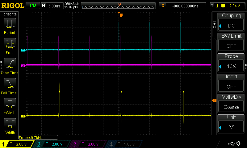
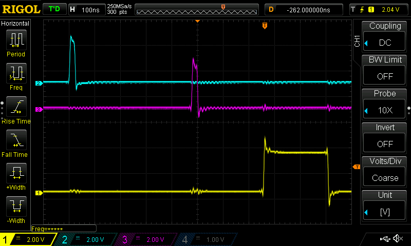
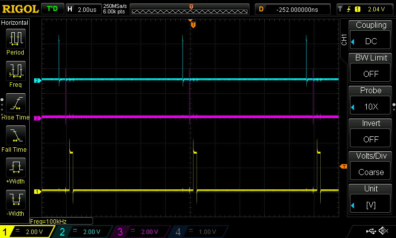
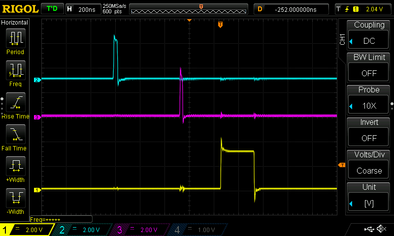
3.) I set up some debug pins and have some scope plots:
I set the DMA Transfer size to 2. This made seing the signals a bit easier.
YELLOW : This gets toggled in the DMA transfer complete ISR
BLUE : This is the output of SCT0_7, the ADC start signal
PURPLE: I enabled the ADC conversion complete routine. The signal is toggled in the IRQ routine.
Plot 1:
I zoomed out so you could see the signals. You can see everything looks
YELLOW : This gets toggled in the DMA transfer complete ISR
BLUE : This is the output of SCT0_7, the ADC start signal
PURPLE: I enabled the ADC conversion complete routine. The signal is toggled in the IRQ routine.
Plot 2
I zoomed in to see the timings around the conversion start, the ADC complete and the DMA complete routines.
YELLOW : This gets toggled in the DMA transfer complete ISR
BLUE : This is the output of SCT0_7, the ADC start signal
PURPLE: I enabled the ADC conversion complete routine. The signal is toggled in the IRQ routine.
Plot 3
This is the Same as Plot 1 EXCEPT that the DMA transfer is only 1 ADC sample.
YELLOW : This gets toggled in the DMA transfer complete ISR
BLUE : This is the output of SCT0_7, the ADC start signal
PURPLE: I enabled the ADC conversion complete routine. The signal is toggled in the IRQ routine.
Plot 4:
This is Plot 3, just zoomed in around 1 set of pulses.
YELLOW : This gets toggled in the DMA transfer complete ISR
BLUE : This is the output of SCT0_7, the ADC start signal
PURPLE: I enabled the ADC conversion complete routine. The signal is toggled in the IRQ routine.
All of the plots make sense to me. The ADC triggers, it completes and then every 2 samples we get a DMA IRQ.
Let me know if there is anything else to try.... This very mysterious.
Thanks for the help.
- 新着としてマーク
- ブックマーク
- 購読
- ミュート
- RSS フィードを購読する
- ハイライト
- 印刷
- 不適切なコンテンツを報告
Hi Eli,
It seems ADC sample data get lost.
Just one more thing to confirm:
I didn't see you configure ADC's clock source, by default it is the "synchorous mode", using system clock, for your setup, it is the 96MHz from FRO HF.
However, UM stated ADC max clock shall <=72MHz:
• In the synchronous operating mode, this ADC clock is derived from the system clock. In this mode, a programmable divider is included to scale the system clock to the maximum ADC clock rate of 72 MHz.
• In the asynchronous mode, an independent clock source is used as the ADC clock source without any further divider in the ADC. The maximum ADC clock rate is 72 MHz as well. In this mode, the ADC clock frequency must not exceed five times the system clock.
But your code "Chip_ADC_Init(LPC_ADC, ADC_CR_RESOL(3) | ADC_CR_CLKDIV(0));" makes ADC clock the same as system clock.
Later after you set the divider other than 0, make sure ADC trigger rate do not get too fast. E.g., ADC uses 15 clocks to do one 12-bit conversion, this means when divider is set 15, trigger rate must <= 96000 / 16 / 15 = 400kHz.
You may also manually set asynchroous mode by setting bit 8 of ADC CTRL register, and specify a clock source by SYSCON's "ADCCLKSEL" register, you could still use FRO HF as ADC clock source.
If you still meet issues, I'll consult PL apps lead for help.
Best regards
Rocky Song
- 新着としてマーク
- ブックマーク
- 購読
- ミュート
- RSS フィードを購読する
- ハイライト
- 印刷
- 不適切なコンテンツを報告
Hello Rocky:
I am aware of the Synchronous Mode max Clock issue mac clock setting and was always trying to work around it. In the case of a ADC_CR_CLKDIV(15), I set the Match Reload to 1000 in this case. This should put the Trigger rate at 96Khz which gives us plenty of margin. My target sample rate if 640KHz so a ADC_CR_CLKDIV of 2 or 4 should still give me plenty of margin.
I'll take one more look at this to double check but I think I am still in the correct operating envelope.
I have not yet tried the asynchronous clock mode. I saw a not that there could be some non-determinism in the conversion start when using this mode. I will give this a try and see if there is any different. I will be away this weekend you might not see a response until next week.
-Eli
- 新着としてマーク
- ブックマーク
- 購読
- ミュート
- RSS フィードを購読する
- ハイライト
- 印刷
- 不適切なコンテンツを報告
Hi Eli,
If you reduce the linked descriptor count to 2 it is ping-pong mode.
I do not have your setup immediately, but for a quick response, could try below testings:
1. Use different (larger) transfer size, e.g., 64. (DMA_TRANSFER_SIZE)
2. Just link the first 2 descriptors to see if the issue remains
3. Use slower ADC clock by changing "ADC_CR_CLKDIV(0)" to "ADC_CR_CLKDIV(15,63,127,255)", and/or "Chip_SCT_SetMatchReload(LPC_SCT, SCT_MATCH_0, 150);", change to larger match reload?
4. Instead of using DAT1, use SEQA global data register. This means you don't use "ADC_SEQ_CTRL_MODE_EOS" to make ADC trigger DMA at every sample, and the DMA source address from "(uint32_t)&LPC_ADC->DAT[1];" change to "(uint32_t)&LPC_ADC->SEQA_GDAT"
And BTW, I see "Initial_DMA_Descriptor.next = (uint32_t)&ADC_TransferDescriptors[0];", seems not the same as
/*
*
* +------------+
* | Initial | Next
* | +------------+
* | Descriptor | |
* +------------+ |
* |
* +------------+ +-----v------+ +------------+ +------------+
* | ADC | Next | ADC | Next | ADC | Next | ADC | Next
* +-----> Descriptor +------> Descriptor +------> Descriptor +------> Descriptor +-----+
* | | 0 | | 1 | | 2 | | 3 | |
* | +------------+ +------------+ +------------+ +------------+ |
* | |
* | |
* +------------------------------------------------------------------------------------+
*
*/Is it "Initial_DMA_Descriptor.next = (uint32_t)&ADC_TransferDescriptors[1];" ?
Best regards
Rocky Song
