- Forums
- Product Forums
- General Purpose MicrocontrollersGeneral Purpose Microcontrollers
- i.MX Forumsi.MX Forums
- QorIQ Processing PlatformsQorIQ Processing Platforms
- Identification and SecurityIdentification and Security
- Power ManagementPower Management
- Wireless ConnectivityWireless Connectivity
- RFID / NFCRFID / NFC
- Advanced AnalogAdvanced Analog
- MCX Microcontrollers
- S32G
- S32K
- S32V
- MPC5xxx
- Other NXP Products
- S12 / MagniV Microcontrollers
- Powertrain and Electrification Analog Drivers
- Sensors
- Vybrid Processors
- Digital Signal Controllers
- 8-bit Microcontrollers
- ColdFire/68K Microcontrollers and Processors
- PowerQUICC Processors
- OSBDM and TBDML
- S32M
- S32Z/E
-
- Solution Forums
- Software Forums
- MCUXpresso Software and ToolsMCUXpresso Software and Tools
- CodeWarriorCodeWarrior
- MQX Software SolutionsMQX Software Solutions
- Model-Based Design Toolbox (MBDT)Model-Based Design Toolbox (MBDT)
- FreeMASTER
- eIQ Machine Learning Software
- Embedded Software and Tools Clinic
- S32 SDK
- S32 Design Studio
- GUI Guider
- Zephyr Project
- Voice Technology
- Application Software Packs
- Secure Provisioning SDK (SPSDK)
- Processor Expert Software
- Generative AI & LLMs
-
- Topics
- Mobile Robotics - Drones and RoversMobile Robotics - Drones and Rovers
- NXP Training ContentNXP Training Content
- University ProgramsUniversity Programs
- Rapid IoT
- NXP Designs
- SafeAssure-Community
- OSS Security & Maintenance
- Using Our Community
-
- Cloud Lab Forums
-
- Knowledge Bases
- ARM Microcontrollers
- i.MX Processors
- Identification and Security
- Model-Based Design Toolbox (MBDT)
- QorIQ Processing Platforms
- S32 Automotive Processing Platform
- Wireless Connectivity
- CodeWarrior
- MCUXpresso Suite of Software and Tools
- MQX Software Solutions
- RFID / NFC
- Advanced Analog
-
- NXP Tech Blogs
- Home
- :
- ARM Microcontrollers
- :
- LPC Microcontrollers Knowledge Base
- :
- LPC's System Clocks
LPC's System Clocks
- Subscribe to RSS Feed
- Mark as New
- Mark as Read
- Bookmark
- Subscribe
- Printer Friendly Page
- Report Inappropriate Content
LPC's System Clocks
LPC's System Clocks
This document describes the different source clocks and the main modules that manage which clock source is used to derive the system clocks that exists on LPC’s devices.
It’s important to know the different clock sources available on our devices, modifying the default clock configuration may have different purposes since increasing the processor performance, achieving specific baud rates for serial communications, power saving, or simply getting a known base reference for a clock timer.
The hardware used for this document is the following:
- LPC: LPCXpresso55S69
Keep in mind that the described hardware and management clock modules in this document are a general overview of the different platforms and the devices listed above are used as a reference example, some terms and hardware modules functionality may vary between devices of the same platform. For more detailed information about the device hardware modules, please refer to your specific device Reference Manual.
LPC platforms
The System Control Block (SYSCON) facilitates the clock generation in the LPC platforms, many clocking variations are possible and the maximum clock frequency for an LPC55S6x platform is @150MHz.
For example, the LPC55S69 device supports 2 external and 3 internal clock sources.
· External Clock Sources
- Crystal oscillator with an operating frequency of 1 MHz to 32 MHz.
- RTC Crystal oscillator with 32.768 kHz operating frequency.
· Internal Clock Sources
- Internal Free Running Oscillator (FRO). This oscillator provides a selectable 96 MHz output, and a 12 MHz output (divided down from the selected higher frequency) that can be used as a system clock.
These 96MHz and 12MHz output frequencies come from a Free Running Oscillator of 192MHz. The 12MHz output provides the default clock at reset and provides a clean system clock shortly after the supply pins reach operating voltage.
Note that the 96MHz clock can only be used for a USB device and is not reliable for USB host timing requirements of the data signaling rate.
- 32 kHz Internal Free Running Oscillator FRO.
The FRO is trimmed to +/- 2% accuracy over the entire voltage and temperature range. This FRO can be enabled in several power-down modes such as Deep-Sleep mode, Power-Down mode, and Deep power-down mode, also is used as a clock source for the 32-bit Real-time clock (RTC).
- Internal low power oscillator (FRO 1 MHz).
The accuracy of this clock is limited to +/- 15% over temperature, voltage, and silicon processing variations after trimming made during assembly. This FRO can be enabled in Deep-Sleep mode, used as a clock source for the PLL0 & PLL1, and for the WWDT(Windowed Watchdog Timer).
The LPC55S69 can achieve up to 150MHz but the clock sources are slower than the final System Clock frequency (@150MHz), inside the SYSCON block two Phase Loop Locked (PLL0 & PLL1) allow CPU operation up to the maximum CPU rate without the need for a high-frequency external clock.
These PLLs can run from the Internal FRO @12 MHz, the external oscillator, internal FRO @1 MHz, or the 32.768 kHz RTC oscillator. These multiple source clocks fit with the required PLL frequency thanks to the wide input frequency range of 2kHz to 150 MHz. The PLLs can be enabled or disabled by software.
The following diagram shows a high-level description of the possible internal and external clock sources, the interaction with the SYSCON block, and the PLL modules.

SYSCON manages the clock sources that will be used for the main clock, system clock, and peripherals.
A clock source is selected and depending on the application to develop the PLL modules are used and configured to perform the desired clock frequency.
Also, the SYSCON module has several clock multiplexors for each peripheral of the board i.e(Systick, FullSpeed-USB, CTimer), so each peripheral can select its source clock regardless of the clock source selection of other peripherals. For example, the following figure shows these described multiplexers and all the possible clock sources that can be used at the specific module.

For more detailed information, refer to “Chapter 4. System Control (SYSCON)” from the LPC55S6x User Manual.
Example: Enabling/Disabling PLLs
The Clock tools available in MCUXpresso IDE, allows you to understand and configure the clock source for the peripherals in the platform. The following diagram shows the default PLL mode configured @150MHz, the yellow path shows all the internal modules involved in the clock configuration.

For example, you can use the Clock tools to configure the clock source of the PLL to use the clk_in coming from the internal 32MHz crystal oscillator, the PLL is configured in bypass mode, therefore the PLL gets inactive resulting in power saving.

For more detailed information about PLL configuration, refer to “Chapter 4.6.6. PLL0 and PLL1 functional description” from the LPC55S6x User Manual.
Example: The next steps describe how to select a clock source for a specific peripheral using Clock Tools.
1.1 Configure clock for specific peripheral
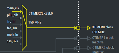
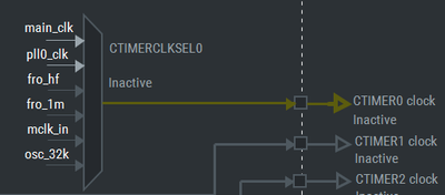
To configure a peripheral as shown in figure 17, Clock Tools is also useful to configure the clock source for the desired peripheral. For example, using the CTimer0 the available clock sources are the following:
- Main Clock
- PLL0 Clock
- FRO 96MHz Clock
- FRO 1MHz Clock
- MCLK Clock
- Oscillator 32KHz Clock
- No Clock(Inactive)
Figure 5. CTimer0 Clock Source Selector
Select CTIMERCLKSEL0 multiplexor and then switch to one of the mentioned clock sources, for example, the main_clk(Main Clock @150MHz) the clock multiplexor gets active and the yellow path is highlighted as shown in the following image.

1.2 Export clock configuration to the project
After you complete the clock configuration, the Clock Tool will update the source code in clock_config.c and clock_config.h, including all the clock functional groups that we created with the tool. This will include the clock source for specific peripherals.
In the previous example, we configured the CTimer0 to use the main_clk; this is translated to the following instruction in source code: “CLOCK_AttachClk(kMAIN_CLK_to_CTIMER0);” inside the “BOARD_BootClockPLL150M();” function.

Note. Remember that before configuring any internal register of a peripheral, its clock source needs to be attached, otherwise, a hard fault occurs.
References
LPC55S6x/LPC55S2x/LPC552x User Manual
Also visit
