- Forums
- Product Forums
- General Purpose MicrocontrollersGeneral Purpose Microcontrollers
- i.MX Forumsi.MX Forums
- QorIQ Processing PlatformsQorIQ Processing Platforms
- Identification and SecurityIdentification and Security
- Power ManagementPower Management
- Wireless ConnectivityWireless Connectivity
- RFID / NFCRFID / NFC
- Advanced AnalogAdvanced Analog
- MCX Microcontrollers
- S32G
- S32K
- S32V
- MPC5xxx
- Other NXP Products
- S12 / MagniV Microcontrollers
- Powertrain and Electrification Analog Drivers
- Sensors
- Vybrid Processors
- Digital Signal Controllers
- 8-bit Microcontrollers
- ColdFire/68K Microcontrollers and Processors
- PowerQUICC Processors
- OSBDM and TBDML
- S32M
- S32Z/E
-
- Solution Forums
- Software Forums
- MCUXpresso Software and ToolsMCUXpresso Software and Tools
- CodeWarriorCodeWarrior
- MQX Software SolutionsMQX Software Solutions
- Model-Based Design Toolbox (MBDT)Model-Based Design Toolbox (MBDT)
- FreeMASTER
- eIQ Machine Learning Software
- Embedded Software and Tools Clinic
- S32 SDK
- S32 Design Studio
- GUI Guider
- Zephyr Project
- Voice Technology
- Application Software Packs
- Secure Provisioning SDK (SPSDK)
- Processor Expert Software
- Generative AI & LLMs
-
- Topics
- Mobile Robotics - Drones and RoversMobile Robotics - Drones and Rovers
- NXP Training ContentNXP Training Content
- University ProgramsUniversity Programs
- Rapid IoT
- NXP Designs
- SafeAssure-Community
- OSS Security & Maintenance
- Using Our Community
-
- Cloud Lab Forums
-
- Knowledge Bases
- ARM Microcontrollers
- i.MX Processors
- Identification and Security
- Model-Based Design Toolbox (MBDT)
- QorIQ Processing Platforms
- S32 Automotive Processing Platform
- Wireless Connectivity
- CodeWarrior
- MCUXpresso Suite of Software and Tools
- MQX Software Solutions
- RFID / NFC
- Advanced Analog
-
- NXP Tech Blogs
- Home
- :
- ARM Microcontrollers
- :
- Kinetisマイクロコントローラ・ナレッジ・ベース
- :
- Kinetis System Clocks
Kinetis System Clocks
- RSS フィードを購読する
- 新着としてマーク
- 既読としてマーク
- ブックマーク
- 購読
- 印刷用ページ
- 不適切なコンテンツを報告
Kinetis System Clocks
Kinetis System Clocks
This document describes the different source clocks and the main modules that manage which clock source is used to derive the system clocks that exists on the Kinetis devices.
It’s important to know the different clock sources available on our devices, modifying the default clock configuration may have different purposes since increasing the processor performance, achieving specific baud rates for serial communications, power saving, or simply getting a known base reference for a clock timer.
The hardware used for this document is the following:
- Kinetis: FRDM-K64F
Keep in mind that the described hardware and management clock modules in this document are a general overview of the different platforms and the devices listed above are used as a reference example, some terms and hardware modules functionality may vary between devices of the same platform. For more detailed information about the device hardware modules, please refer to your specific device Reference Manual.
Kinetis platforms
The Kinetis devices have a main module called Multipurpose Clock Generator (MCG) this module controls which clock source is used to derive the system clocks. A high-level description diagram is shown below:
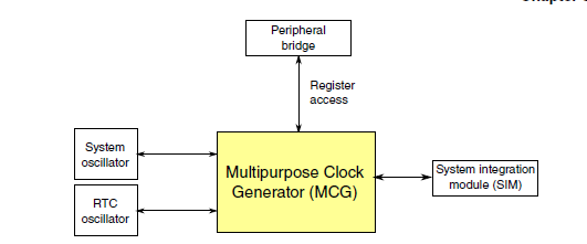
External clock sources can provide a frequency signal as the System oscillator module or the RTC oscillator module, also the MCG module has internal clock generators that the System integration module (SIM) manages, the SIM module provides module-specific clock gating to allow granular shutoff of modules.
For more detailed information about the SIM module, refer to “Chapter 12. System Integration Module(SIM)” from the K64 Sub-Family Reference Manual.
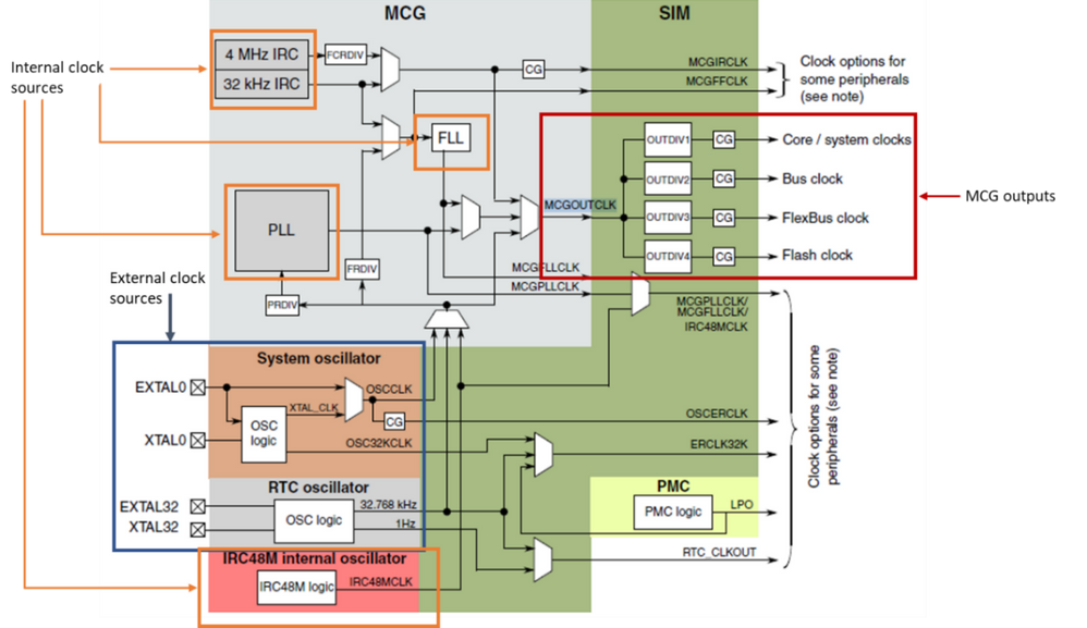
The following clock diagram shows all the multiplexers, dividers, and clock gates that can be controlled by the MCG, however, we will focus on the external and internal clock sources and the MCG outputs.
Figure 2. Oscillators, MCG and SIM modules
At ‘MCGOUTCLK’ line, the primary clocks for the system are generated, the circuitry provides fixed clock dividers for the Core clock, Bus clock, FlexBus clock, and the Flash Clock. This allows for trade-offs between performance and power dissipation.
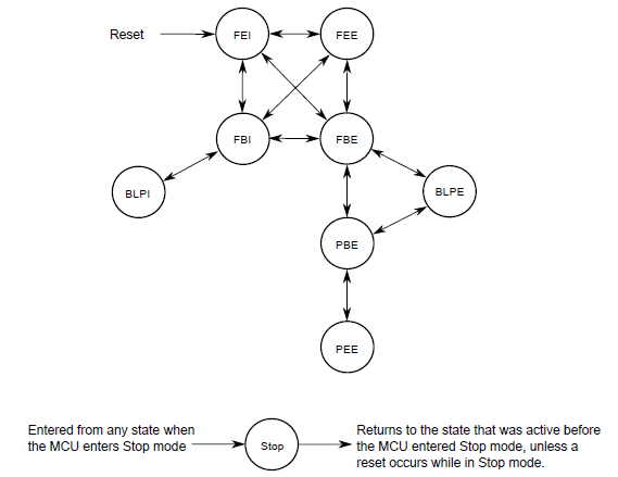
It’s important to know that the MCG has 9 states of operation shown in the following figure.
Figure 3. MCG operation states
In the previous image, the arrows indicate the permitted MCG state transitions, for example, if the current MCG state is BLPI(Bypassed Low Power Internal) and the desired state is BLPE(Bypassed Low Power External) the shortest and allowed path to follow is first switch to FBI(FLL Bypassed Internal) then to FBE(FLL Bypassed External), and finally to the BLPE MCG state. These switching mode restrictions exist due to certain MCG configuration bits that must be changed to properly move from one mode to another.
For example, in the K64 family, the MCG state after a power-on reset is FEI(FLL Engaged Internal) mode, the MCGOUTCLK is derived from the FLL clock that is controlled by the 32kHz Internal Reference Clock (IRC), the following table shows the output frequency values for this specific MCG state.
|
Source |
Frequency |
|
MCGOUTCLK |
20.97MHZ |
|
Core/System clocks |
20.97MHz |
|
Bus clock |
10.48MHz |
|
FlexBus clock |
6.99MHz |
|
Flash clock |
4.19MHz |
Table 1. K64 default MCG configuration after reset: FEI (FLL Engaged Internal)
The following image shows the blocks used for the FEI state using Clocks Tool from MCUXpresso IDE.

For more detailed information, refer to “Chapter 25. Multipurpose Clock Generator (MCG)” from the K64 Sub-Family Reference Manual.
- External Clock Sources
- System oscillator
The System Oscillator module is a crystal oscillator. The module, in conjunction with an external crystal or resonator, generates a reference clock for the MCU. Supports 32 kHz crystals (Low Range mode) and supports 3–8 MHz, 8–32 MHz crystals and resonators (High Range mode)
For more detailed information, refer to Chapter 26. Oscillator(OSC) at K64 Sub-Family Reference Manual.
- RTC oscillator
The RTC oscillator module, in conjunction with an external crystal, generates a reference clock source of 1Hz and 32.768KHz, supports 32 kHz crystals with very low power.
For more detailed information, refer to Chapter 27. RTC Oscillator(OSC32K) at K64 Sub-Family Reference Manual.
- Internal Clock Sources
- IRC oscillators
Internal clock driven by the Fast Internal Reference (FIR) @4MHz or the Slow Internal Reference (SIR) @32kHz.
- IRC internal oscillator
Internal 48 MHz oscillator that can be used as a reference to the MCG and also may clock some on-chip modules.
- PLL
Phase-locked loop circuit that in conjunction with an external clock source can achieve higher and stable frequencies.
- FLL
Frequency-locked loop circuit that in conjunction with an internal/external clock source provides module-specific clock and achieves higher frequencies.
Modifying MCG state from FEI to FBI state
If the current system clock does not fit with our timing requirements we can modify it by changing the state of the MCG module, in this case, if the user requires a lower system clock frequency @32.7KHz(Slow IRC) or @4MHz(Fast IRC) instead @21MHz(FLL Engaged Internal ‘FEI’ default state) and a low power option of the MCG module, the FLL Bypass Internal (FBI) state is an option to reach these requirements.
1.1 Configure MCG mode
The FBI state allows us to use the Fast IRC together with its frequency divider achieving frequencies between 31.25KHz to 4MHz, for this example the final core clock is @2MHz. Follow the next steps to change to the FBI state and select a 2MHz clock using the Clock-Tools tool from MCUXpresso IDE.
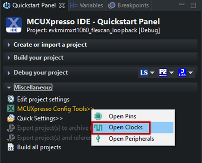
- At the MCUXpresso QuickStart Panel select MCUXpresso Config Tools >> Open Clocks
- At the left top of the screen select the MCG mode to “FBI(FLL Bypassed Internal)”

- Select the frequency divider block(FCRDIV) right-click on it and select “Edit settings of: FCRDIV”

- Modify the divider value from 1 to 2.

- Finally, the next image shows how the MCG state and the new yellow paths get modified. The Core and system clocks are @2MHz.

1.2 Export clock configuration to the project
After you complete the clock configuration, the Clock Tool will update the source code in clock_config.c and clock_config.h, including all the clock functional groups that we created with the tool. In the previous example, we configured the MCG state to FBI mode, this is translated to the following instructions in source code: “CLOCK_SetInternalRefClkConfig();” and “CLOCK_SetFbiMode();”

Another way to change the MCG state is by directly modifying the internal MCG registers. The blocks shown in the following image need to be modified to switch from the default FEI state to the FBI state.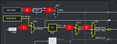
Note. MCG registers can only be written in supervisor mode. The ARM core runs in privileged(supervisor mode) out of reset, it is controlled by [nPRIV] bit in CONTROL core register. For more detailed information visit the Cortex-M4 ARM Documentation Reference Manual.
- Internal Reference Source Multiplexor (IREFS), selects the reference source clock for the FLL.
- 1 is written to C1[IREFS].
- The slow internal reference is selected.
- PLL Select Multiplexor(PLLS) Controls whether the PLL or FLL output is selected.
- 0 is written to C6[PLLS]
- The FLL output is selected as the MCG source, the PLL is disabled.
- Clock Source Select Multiplexor(CLKS), selects the clock source for the MCGOUTCLK line.
- 01 is written to C1[CLKS].
- The internal reference clock is selected at the CLKS multiplexor.
- Fast Clock Internal Reference Divider(FCRDIV), selects the Fast Internal Reference Clock divider, the resulting frequency can be in the range of 31.25KHz to 4MHz.
- 001 is written to SC[FCRDIV].
- The dividing factor is 2 since the desired frequency is @2MHz and the source clock is @4MHz.
- Internal Reference Clock Select (IRCS). Selects between the fast or slow internal reference clock source.
- x is written to C2[IRCS].
- Write 0 for Slow IRC or 1 for Fast IRC.
- Finally, to enable the low power when neither the PLL nor FLL are used, a register in C2[LP] is modified.
- x is written to C2[LP].
- Enable, or Disable the PLL & FLL in all the bypass modes.
This is translated to the following instructions in source code in “CLOCK_SetInternalRefClkConfig();” and “CLOCK_SetFbiMode();” functions:
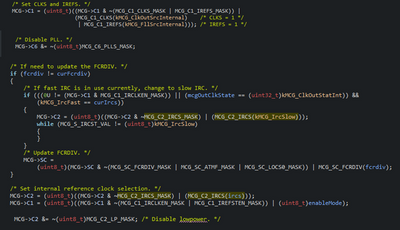
Note. C1, C2, C6, and SC registers are part of the internal MCG control registers.
References
K64 Sub-Family Reference Manual
Also visit
