- Forums
- Product Forums
- General Purpose MicrocontrollersGeneral Purpose Microcontrollers
- i.MX Forumsi.MX Forums
- QorIQ Processing PlatformsQorIQ Processing Platforms
- Identification and SecurityIdentification and Security
- Power ManagementPower Management
- MCX Microcontrollers
- S32G
- S32K
- S32V
- MPC5xxx
- Other NXP Products
- Wireless Connectivity
- S12 / MagniV Microcontrollers
- Powertrain and Electrification Analog Drivers
- Sensors
- Vybrid Processors
- Digital Signal Controllers
- 8-bit Microcontrollers
- ColdFire/68K Microcontrollers and Processors
- PowerQUICC Processors
- OSBDM and TBDML
- S32M
-
- Solution Forums
- Software Forums
- MCUXpresso Software and ToolsMCUXpresso Software and Tools
- CodeWarriorCodeWarrior
- MQX Software SolutionsMQX Software Solutions
- Model-Based Design Toolbox (MBDT)Model-Based Design Toolbox (MBDT)
- FreeMASTER
- eIQ Machine Learning Software
- Embedded Software and Tools Clinic
- S32 SDK
- S32 Design Studio
- GUI Guider
- Zephyr Project
- Voice Technology
- Application Software Packs
- Secure Provisioning SDK (SPSDK)
- Processor Expert Software
- MCUXpresso Training Hub
-
- Topics
- Mobile Robotics - Drones and RoversMobile Robotics - Drones and Rovers
- NXP Training ContentNXP Training Content
- University ProgramsUniversity Programs
- Rapid IoT
- NXP Designs
- SafeAssure-Community
- OSS Security & Maintenance
- Using Our Community
-
- Cloud Lab Forums
-
- Knowledge Bases
- ARM Microcontrollers
- i.MX Processors
- Identification and Security
- Model-Based Design Toolbox (MBDT)
- QorIQ Processing Platforms
- S32 Automotive Processing Platform
- Wireless Connectivity
- CodeWarrior
- MCUXpresso Suite of Software and Tools
- MQX Software Solutions
-
- Home
- :
- General Purpose Microcontrollers
- :
- Kinetis Microcontrollers
- :
- Re: LCDC 16bpp question and frame buffer structure
LCDC 16bpp question and frame buffer structure
- Subscribe to RSS Feed
- Mark Topic as New
- Mark Topic as Read
- Float this Topic for Current User
- Bookmark
- Subscribe
- Mute
- Printer Friendly Page
- Mark as New
- Bookmark
- Subscribe
- Mute
- Subscribe to RSS Feed
- Permalink
- Report Inappropriate Content
Hi
I am trying to get 800x480 display to run in 16bpp mode, and can also make it work. But It seems like the frame buffer has to be interleaved after each Hsync. Meaning that I have to make my frame buffer twice the size.
Can that be the case our is the DMA settings not correct?
I have modified the lcdc example from SC to the following setting:
lcdc.h (buffer size adjusted + screen resolution):
#define SCREEN_XSIZE 800 //PEILNI: changed to 800x480
#define SCREEN_YSIZE 480
#define GW_XSIZE (SCREEN_XSIZE/2)
#define GW_YSIZE (SCREEN_YSIZE/2)

#define FRAME_START_ADDRESS 0x80400000 //Screen in DDR
#define GW_START_ADDRESS 0x80200000

#define FRAME_BUFFER_SIZE (SCREEN_XSIZE * SCREEN_YSIZE * 2) //4 bytes per pixel for 24bpp //PEILNI: changed to 2 bytes since we use 16 bpp
#define GW_BUFFER_SIZE (GW_XSIZE * GW_YSIZE * 2) //4 bytes per pixel for 24bpp //PEILNI: changed to 2 bytes since we use 16 bpp
And some in lcdc.c, this is timing for the display and from 24bpp to 16bpp:
// set LCD panel configuration. Use endianess to work with TWR-LCD-RGB lines.
  LCDC_LPCR =
  LCDC_LPCR_TFT_MASK | //TFT Screen
  LCDC_LPCR_COLOR_MASK | //Color
  LCDC_LPCR_BPIX(0x5) | //24 bpp //PEILNI:changed to 16bpp
  LCDC_LPCR_FLMPOL_MASK | //first line marker active low (VSYNC)
  LCDC_LPCR_LPPOL_MASK | //line pulse active low (HSYNC)
  LCDC_LPCR_END_SEL_MASK | //Use big-endian mode (0xFFAA5500 means R=AA,G=55,B=00).
  //LCDC_LPCR_SWAP_SEL_MASK | //Set if needed for LCD data lines match up correctly with the LCD
  LCDC_LPCR_SCLKIDLE_MASK | //Enalbe LSCLK when vsync is idle
  LCDC_LPCR_SCLKSEL_MASK | //Always enable clock
  LCDC_LPCR_PCD(3); //PEILNI: changed from 11 to 3 to 30MHz clock//Divide 120 PLL0 clock (default clock) by (11+1)=12 to get 10MHz clock


  LCDC_LPCR |= LCDC_LPCR_CLKPOL_MASK; //In TFT mode, active on negative edge of LSCLK.

  // set LCD horizontal configuration based on panel data (Figure 3-3 in Seiko datasheet)
  LCDC_LHCR =
  LCDC_LHCR_H_WIDTH(0) | //(41+1)=42 SCLK period for HSYNC activated//PEILNI: changed to fit display timing
  LCDC_LHCR_H_WAIT_1(191) | //(1+1)=2 SCLK period between end of OE and beginning of HSYNC //PEILNI: changed to fit display timing
  LCDC_LHCR_H_WAIT_2(0); //(0+3)=3 SCLK periods between end of HSYNC and beginning of OE

  // set LCD vertical configuration based on panel data (Figure 3-3 in Seiko datasheet)

  LCDC_LVCR =
  LCDC_LVCR_V_WIDTH(0) | //2 lines period for VSYNC activated //PEILNI: changed to fit display timing
  LCDC_LVCR_V_WAIT_1(20) | //1 line period between end of OE and beginning of VSYNC //PEILNI: changed to fit display timing
  LCDC_LVCR_V_WAIT_2(1); //1 line periods between end of VSYNC and beginning of OE
And aldo lcdc_color.c. In order to fit the new 16bpp color scheme. see the comment in line 06 and line 25
uint16_t *pointer16;
  int i,n;

pointer16=(uint16_t *)FRAME_START_ADDRESS;
//Loop through top half of screen
  for(i=0;i<SCREEN_YSIZE/1;i++) //PEILNI: in order to get to work this size has to double then expected?
  {
  //One half will be white
  for(n=0;n<SCREEN_XSIZE/2;n++)
  {
  *pointer16=0xFFFF; //White
  pointer16++;
  }

  //One half will be blue
  for(n=0;n<SCREEN_XSIZE/2;n++)
  {
  *pointer16=0x001F; //Blue

  pointer16++;
  }
  }

  //Loop through bottom half of screen
  for(i=0;i<SCREEN_YSIZE/1;i++)  //PEILNI: in order to get to work this size has to double then expected?
  {
  //One half will be blue
  for(n=0;n<SCREEN_XSIZE/2;n++)
  {
  //*pointer32=0x000000FF; //Blue
  *pointer16=0x07e0; //Green
  pointer16++;
  }

  // One half will be white
  for(n=0;n<SCREEN_XSIZE/2;n++)
  {
  *pointer16=0xf800; //Red
  pointer16++;
  }
  }

  /* Create a graphic window filled with the color black*/
  pointer16=(uint16_t *)GW_START_ADDRESS;
  for(i=0;i<GW_BUFFER_SIZE/2;i++)
  {
  *pointer16= 0x2B50; //something
  pointer16++;
  }
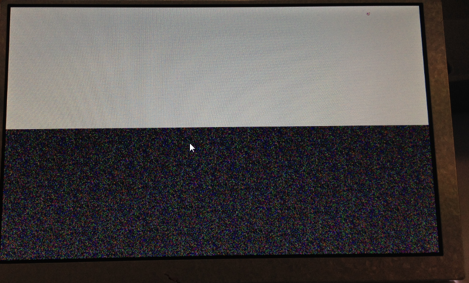
If I do not add twice as many bytes in the frame buffer (see line 06 and 25 above) I only get half the display see picture(halfScreen.jpg) and if I make the buffer double size (fullScreen.jpg) :
Hope for some help.
Br. Peter Ilsoe
Solved! Go to Solution.
- Mark as New
- Bookmark
- Subscribe
- Mute
- Subscribe to RSS Feed
- Permalink
- Report Inappropriate Content
Hi
The solution was to set the virtual page correct up. My new best friend Martin has spotted that the virtual page is in 32 bit words:

Meaning that the virtual page should only be half the size.
// set LCD virtual page width
LCDC_LVPWR = LCDC_LVPWR_VPW( SCREEN_XSIZE/2 ); //Peilni: this number is in 32 bit words, since we use 16 bpp is should be the half siz
Best regards Peter Ilsoe
- Mark as New
- Bookmark
- Subscribe
- Mute
- Subscribe to RSS Feed
- Permalink
- Report Inappropriate Content
Hi Peter,
would you please share the panel data sheet for a review? Thanks for your patience!!
Have a great day!
B.R
Kan
- Mark as New
- Bookmark
- Subscribe
- Mute
- Subscribe to RSS Feed
- Permalink
- Report Inappropriate Content
Hi Kan,
We have following setup:
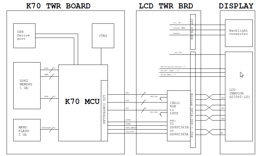
K70 (16 pins) -> LVDS controller -> LCD Display. See block diagram:
The data sheet for the panel/display:
http://www.data-modul.com/tl_files/dm/data/specification_BT63170.pdf_
B.R.
Peter Ilsoe
- Mark as New
- Bookmark
- Subscribe
- Mute
- Subscribe to RSS Feed
- Permalink
- Report Inappropriate Content
Hi Peter,
Thanks for the information!! I am investigating these, and how about the image map? I mean what is the location for the code section, data section and LCD frame buffer? You mentioned the project is from lcdc demo, so did you apply the Flash_1M? or DDR2_128M? Please kindly help to clarify!!
Have a nice day!
B.R
Kan
- Mark as New
- Bookmark
- Subscribe
- Mute
- Subscribe to RSS Feed
- Permalink
- Report Inappropriate Content
Hi Kan,
I applied DDR_128M. And the location is for the BMP image is see map file with bold:
Entry Address Size Type Object
----- ------- ---- ---- ------
.bss$$Base 0x085783f8 -- Gb - Linker created -
.bss$$Limit 0x08578410 -- Gb - Linker created -
.data$$Base 0x00000000 -- Gb - Linker created -
.data_init$$Base 0x00000000 -- Gb - Linker created -
.data_init$$Limit 0x00000000 -- Gb - Linker created -
?main 0x08578195 Code Gb cmain.o [5]
CodeRelocate$$Base 0x085783f8 -- Gb - Linker created -
CodeRelocate$$Limit 0x085783f8 -- Gb - Linker created -
CodeRelocateRam$$Base 0x08578410 -- Gb - Linker created -
CodeRelocateRam$$Limit 0x08578410 -- Gb - Linker created -
Region$$Table$$Base 0x08578078 -- Gb - Linker created -
Region$$Table$$Limit 0x08578088 -- Gb - Linker created -
__BOOT_STACK_ADDRESS {Abs}
0x0ffffff8 -- Gb command line/config [2]
__VECTOR_RAM {Abs} 0x1fff0000 -- Gb command line/config [2]
__VECTOR_TABLE {Abs} 0x1fff0000 -- Gb command line/config [2]
__cmain 0x08578195 Code Gb cmain.o [5]
__exit 0x085781c5 0x14 Code Gb exit.o [6]
__iar_data_init3 0x0857802d 0x28 Code Gb data_init.o [5]
__iar_init_vfp 0x08578179 Code Gb fpinit_M.o [4]
__iar_program_start 0x085783c5 Code Gb cstartup_M.o [5]
__iar_zero_init3 0x085774ef 0x22 Code Gb zero_init3.o [5]
__low_level_init 0x085781af 0x4 Code Gb low_level_init.o [3]
__mla 0x08000455 Code Gb dsp_asm.o [1]
__smlabb 0x08000467 Code Gb dsp_asm.o [1]
__smlabt 0x0800046d Code Gb dsp_asm.o [1]
__smlad 0x0800047f Code Gb dsp_asm.o [1]
__smladx 0x08000485 Code Gb dsp_asm.o [1]
__smlal 0x0800045b Code Gb dsp_asm.o [1]
__smlalbb 0x0800048b Code Gb dsp_asm.o [1]
__smlalbt 0x08000491 Code Gb dsp_asm.o [1]
__smlald 0x080004a3 Code Gb dsp_asm.o [1]
__smlaldx 0x080004a9 Code Gb dsp_asm.o [1]
__smlaltb 0x08000497 Code Gb dsp_asm.o [1]
__smlaltt 0x0800049d Code Gb dsp_asm.o [1]
__smlatb 0x08000473 Code Gb dsp_asm.o [1]
__smlatt 0x08000479 Code Gb dsp_asm.o [1]
__smlawb 0x080004af Code Gb dsp_asm.o [1]
__smlawt 0x080004b5 Code Gb dsp_asm.o [1]
__smlsd 0x080004bb Code Gb dsp_asm.o [1]
__smlsdx 0x080004c1 Code Gb dsp_asm.o [1]
__smlsld 0x080004c7 Code Gb dsp_asm.o [1]
__smlsldx 0x080004cd Code Gb dsp_asm.o [1]
__smmla 0x080004d3 Code Gb dsp_asm.o [1]
__smmlar 0x080004d9 Code Gb dsp_asm.o [1]
__smmls 0x080004df Code Gb dsp_asm.o [1]
__smmlsr 0x080004e5 Code Gb dsp_asm.o [1]
__smmul 0x080004eb Code Gb dsp_asm.o [1]
__smmulr 0x080004f1 Code Gb dsp_asm.o [1]
__smuad 0x080004f7 Code Gb dsp_asm.o [1]
__smuadx 0x080004fd Code Gb dsp_asm.o [1]
__smulbb 0x08000503 Code Gb dsp_asm.o [1]
__smulbt 0x08000509 Code Gb dsp_asm.o [1]
__smull 0x08000461 Code Gb dsp_asm.o [1]
__smultb 0x0800050f Code Gb dsp_asm.o [1]
__smultt 0x08000515 Code Gb dsp_asm.o [1]
__smulwb 0x0800051b Code Gb dsp_asm.o [1]
__smulwt 0x08000521 Code Gb dsp_asm.o [1]
__smusd 0x08000527 Code Gb dsp_asm.o [1]
__smusdx 0x0800052d Code Gb dsp_asm.o [1]
__startup 0x08000411 Code Gb crt0.o [1]
__umaal 0x0800053f Code Gb dsp_asm.o [1]
__umlal 0x08000533 Code Gb dsp_asm.o [1]
__umull 0x08000539 Code Gb dsp_asm.o [1]
__vector_table 0x1fff0000 0x410 Data Gb vectors.o [1]
_call_main 0x085781a1 Code Gb cmain.o [5]
_exit 0x085781b9 Code Gb cexit.o [5]
_main 0x085781ab Code Gb cmain.o [5]
common_startup 0x08577d6d 0x9c Code Gb startup.o [1]
core_clk_khz 0x08578400 0x4 Data Gb sysinit.o [1]
cpu_identify 0x08577b37 0xf8 Code Gb start.o [1]
default_isr 0x08578299 0x18 Code Gb vectors.o [1]
exit 0x085781b3 0x4 Code Gb exit.o [3]
flash_identify 0x08577c2f 0x76 Code Gb start.o [1]
in_char 0x085777b5 0xa Code Gb io.o [1]
lcdc_gallery_demo 0x0857776d 0x48 Code Gb lcdc_gallery.o [1]
lcdc_init_pins 0x0857754b 0xe2 Code Gb lcdc.o [1]
lcdc_init_screen 0x0857762d 0x7a Code Gb lcdc.o [1]
main 0x08577511 0x3a Code Gb lcdc.o [1]
mcg_clk_hz 0x085783f8 0x4 Data Gb sysinit.o [1]
mcg_clk_khz 0x085783fc 0x4 Data Gb sysinit.o [1]
outSRS 0x085778cd 0x1d4 Code Gb rcm.o [1]
out_char 0x085777bf 0xe Code Gb io.o [1]
periph_clk_khz 0x08578404 0x4 Data Gb sysinit.o [1]
pll_0_clk_khz 0x08578408 0x4 Data Gb sysinit.o [1]
pll_1_clk_khz 0x0857840c 0x4 Data Gb sysinit.o [1]
printf 0x085774b1 0x1e Code Gb printf.o [1]
printk 0x085770d9 0x3d8 Code Gb printf.o [1]
printk_mknumstr 0x0857702d 0x70 Code Lc printf.o [1]
printk_pad_space 0x085770bb 0x1e Code Lc printf.o [1]
printk_pad_zero 0x0857709d 0x1e Code Lc printf.o [1]
printk_putc 0x08577001 0x2c Code Lc printf.o [1]
start 0x08577b15 0x22 Code Gb start.o [1]
strlen 0x085774d5 0x1a Code Gb stdlib.o [1]
sysinit 0x08577e09 0x78 Code Gb sysinit.o [1]
testImage24 0x08400000 0x177000 Data Lc lcdc_gallery.o [1]
uart_getchar 0x085778b9 0xa Code Gb uart.o [1]
uart_init 0x085777d1 0xcc Code Gb uart.o [1]
uart_putchar 0x085778c3 0xa Code Gb uart.o [1]
wdog_disable 0x08577d35 0x16 Code Gb wdog.o [1]
wdog_unlock 0x08577d4d 0x16 Code Gb wdog.o [1]
write_vtor 0x08577eb1 0x6 Code Gb arm_cm4.o [1]
Br.
Peter Ilsoe
- Mark as New
- Bookmark
- Subscribe
- Mute
- Subscribe to RSS Feed
- Permalink
- Report Inappropriate Content
Hi Peter,
Thanks for the information!! Actually I just found the following note from the panel DS:
Note (1) Since this assembly is operated in DE only mode, Hsync and Vsync input signals should be set to
low logic level. Otherwise, this assembly would operate abnormally.
While from your diagram of device connection, HSYNC and VSYNC of K70 are connected with LVDS controller, and there would be high state on these two pins during transaction, so I am wondering if you have modified "void lcdc_init_pins()" accordingly. You may find the original code set PTF2 and PTF3 as HSYNC and VSYNC.
PORTF_PCR2=ALT7; // Graphic LCD HSYNC, Schematic PTF2
PORTF_PCR3=ALT7; // Graphic LCD VSYNC, Schematic PTF3
If you still use the original lcdc_init_pins(), please set PTF2 and PTF3 to GPIO function and output low to check if there is any difference after that.
Hope that helps,
Have a great day,
Kan
-----------------------------------------------------------------------------------------------------------------------
Note: If this post answers your question, please click the Correct Answer button. Thank you!
-----------------------------------------------------------------------------------------------------------------------
- Mark as New
- Bookmark
- Subscribe
- Mute
- Subscribe to RSS Feed
- Permalink
- Report Inappropriate Content
Hi Kan,
I have tried to changed them to GPIO no luck:-(
I will try to measure the timing of OE.
Br. Peter
- Mark as New
- Bookmark
- Subscribe
- Mute
- Subscribe to RSS Feed
- Permalink
- Report Inappropriate Content
Hi,
I have tried to measure the timing of OE or DE as the Panel data sheet call it:
From data sheet:
Blanking: (1/30e6)*192 = 6.4us
Measured = 6.5 us
Active: (1/30e6)*800 = 26.67us
Measured = 27us

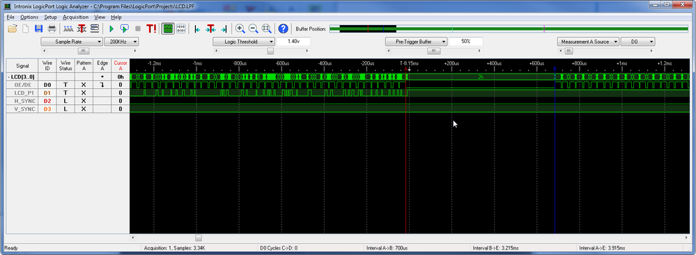
The vertical timing is all so okay see picture:
From data sheet:
Typical timing: (1/30e6) *20*992 = 661.33us
Max: (1/30e6) *20*1090 = 726.67us
Measured: = 700 us
So in my view the timing is okay.
Br. Peter Ilsoe
- Mark as New
- Bookmark
- Subscribe
- Mute
- Subscribe to RSS Feed
- Permalink
- Report Inappropriate Content
Hi Kan,
In order to prof that in 16 bpp mode there is some thing wrong with the DMA burst I have make an example where the frame buffer look like this:
0x08400000 : ff ff ff ff ff ff ff ff ff ff ff ff ff ff ff ff //white
.....
0x08400630 :ff ff ff ff ff ff ff ff ff ff ff ff ff ff ff ff
0x08400640 : 00 00 00 00 00 00 00 00 00 00 00 00 00 00 00 00 //Black
....
0x08400C70 : 00 00 00 00 00 00 00 00 00 00 00 00 00 00 00 00
0x08400C80 :ff ff ff ff ff ff ff ff ff ff ff ff ff ff ff ff
.......................
0x084BB7F0 : 00 00 00 00 00 00 00 00 00 00 00 00 00 00 00 00 //end of frame buffer 768000 bytes (800*480*2)
0x084BB800:60 81 50 5c 40 18 08 cc 26 08 22 e1 55 04 08 80 //Out of frame buffer random data
So I would expect a display showing first a white horizontal line and then a black etc...
But I get: 240 white lines and then 240 random lines see image:

So then is the question if the black lines are outside of the panel. Meaning that they are clocked out after a white line but no horizontal sync? In order to show that this is not the case I monitor LCD_P1 pin (Blue 0). If the black pixels are clocked out one should expect that LCD_P1 should go low after one Hsync (our in my cace one OE/DE cycle). This is not he case see image:
So is there some where I can set the increment of each line burst (DMA burst to LCDC)?
I my view it seems like it increments 32bit*800 and not 16bit*800 for each line in 16bpp mode.
Br. Peter Ilsoe
- Mark as New
- Bookmark
- Subscribe
- Mute
- Subscribe to RSS Feed
- Permalink
- Report Inappropriate Content
Hi
The solution was to set the virtual page correct up. My new best friend Martin has spotted that the virtual page is in 32 bit words:

Meaning that the virtual page should only be half the size.
// set LCD virtual page width
LCDC_LVPWR = LCDC_LVPWR_VPW( SCREEN_XSIZE/2 ); //Peilni: this number is in 32 bit words, since we use 16 bpp is should be the half siz
Best regards Peter Ilsoe
- Mark as New
- Bookmark
- Subscribe
- Mute
- Subscribe to RSS Feed
- Permalink
- Report Inappropriate Content
Hello,
Thank you for your post, however please consider moving it to the right community place (e.g. Kinetis Microcontrollers or Other Freescale Solutions) to get it visible for active members.
For details please see general advice Where to post a Discussion?
Thank you for using Freescale Community.


