- Forums
- Product Forums
- General Purpose MicrocontrollersGeneral Purpose Microcontrollers
- i.MX Forumsi.MX Forums
- QorIQ Processing PlatformsQorIQ Processing Platforms
- Identification and SecurityIdentification and Security
- Power ManagementPower Management
- Wireless ConnectivityWireless Connectivity
- RFID / NFCRFID / NFC
- Advanced AnalogAdvanced Analog
- MCX Microcontrollers
- S32G
- S32K
- S32V
- MPC5xxx
- Other NXP Products
- S12 / MagniV Microcontrollers
- Powertrain and Electrification Analog Drivers
- Sensors
- Vybrid Processors
- Digital Signal Controllers
- 8-bit Microcontrollers
- ColdFire/68K Microcontrollers and Processors
- PowerQUICC Processors
- OSBDM and TBDML
- S32M
- S32Z/E
-
- Solution Forums
- Software Forums
- MCUXpresso Software and ToolsMCUXpresso Software and Tools
- CodeWarriorCodeWarrior
- MQX Software SolutionsMQX Software Solutions
- Model-Based Design Toolbox (MBDT)Model-Based Design Toolbox (MBDT)
- FreeMASTER
- eIQ Machine Learning Software
- Embedded Software and Tools Clinic
- S32 SDK
- S32 Design Studio
- GUI Guider
- Zephyr Project
- Voice Technology
- Application Software Packs
- Secure Provisioning SDK (SPSDK)
- Processor Expert Software
- Generative AI & LLMs
-
- Topics
- Mobile Robotics - Drones and RoversMobile Robotics - Drones and Rovers
- NXP Training ContentNXP Training Content
- University ProgramsUniversity Programs
- Rapid IoT
- NXP Designs
- SafeAssure-Community
- OSS Security & Maintenance
- Using Our Community
-
- Cloud Lab Forums
-
- Knowledge Bases
- ARM Microcontrollers
- i.MX Processors
- Identification and Security
- Model-Based Design Toolbox (MBDT)
- QorIQ Processing Platforms
- S32 Automotive Processing Platform
- Wireless Connectivity
- CodeWarrior
- MCUXpresso Suite of Software and Tools
- MQX Software Solutions
- RFID / NFC
- Advanced Analog
-
- NXP Tech Blogs
- Home
- :
- 汎用マイクロコントローラ
- :
- Kinetisマイクロコントローラ
- :
- Kinetis: cannot enter background mode with P&E GDB server
Kinetis: cannot enter background mode with P&E GDB server
- RSS フィードを購読する
- トピックを新着としてマーク
- トピックを既読としてマーク
- このトピックを現在のユーザーにフロートします
- ブックマーク
- 購読
- ミュート
- 印刷用ページ
- 新着としてマーク
- ブックマーク
- 購読
- ミュート
- RSS フィードを購読する
- ハイライト
- 印刷
- 不適切なコンテンツを報告
Hi,
I try to connect to a custom board using P&E multilink tool and P&E GDB server for Kinetis. My MCU is MK60DN512VMD10.
I get the error message as follows:
Server running on 127.0.0.1:7224
P&E Interface detected - Flash Version 9.33
Can not enter background mode .
Unable to initialize PEDebug.
PE-ERROR: Failed to Initialize Target
I tried to change device name, additional options (SWD mode on/off, erase on connect on/off) and debug speed, but still the same message. When I measure on the JTAG with an oscilloscope, I detect activity on the reset, TCK, TMS and TDI lines. The levels look correct. But there is no activity on TDO!
I don't have an external oscillator in my design. The EZP_CS_b pin is not connected either. Could any of this be the problem?
Regards,
Yulia
解決済! 解決策の投稿を見る。
- 新着としてマーク
- ブックマーク
- 購読
- ミュート
- RSS フィードを購読する
- ハイライト
- 印刷
- 不適切なコンテンツを報告
Hi,
I finally solved it. The schematic was wrong and the pin-out of the JTAG was not correct relative to the HW.
Regards,
Yulia
- 新着としてマーク
- ブックマーク
- 購読
- ミュート
- RSS フィードを購読する
- ハイライト
- 印刷
- 不適切なコンテンツを報告
Hello Yulia,
It usually is due to hardware problems. Could you please share your schematic (at least the debug interface)?
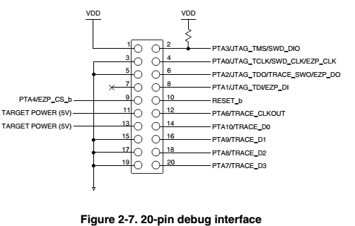
In the KQRUG in the section 2.1.5.3 Debug interface are shown the hardware considerations for the JTAG and SWD interfaces.
There can be seen that the data line needs a pull up resistor. Also, it is needed a pull up resistor and a ~100 nF capacitor in the reset line, this is not shown in those schematics.
Please confirm that you have that hardware in your board.
Beast regards,
Earl Orlando.
- 新着としてマーク
- ブックマーク
- 購読
- ミュート
- RSS フィードを購読する
- ハイライト
- 印刷
- 不適切なコンテンツを報告
Hi Earl Orlando,
thanks for the reply.
My JTAG was originally routed the wrong way but I fixed it in my cable. My configuration is as shown in your figure 2-8 besides pin 9 which is grounded on the connector. The MCU pin EZP_CS_B is floating. I have a 10k pull-up on both JTAG_TMS and reset_b. I have also added a 100n capacitor to ground. Still the same problem.
I have also tried to use the JTAG tool from the KDS on Linux. The debugger detects the tool but debugging fails with the following message:
The board was programmed with some simple code by another company before I got it, but it shouldn't matter, should it?
- 新着としてマーク
- ブックマーク
- 購読
- ミュート
- RSS フィードを購読する
- ハイライト
- 印刷
- 不適切なコンテンツを報告
Hello Yulia,
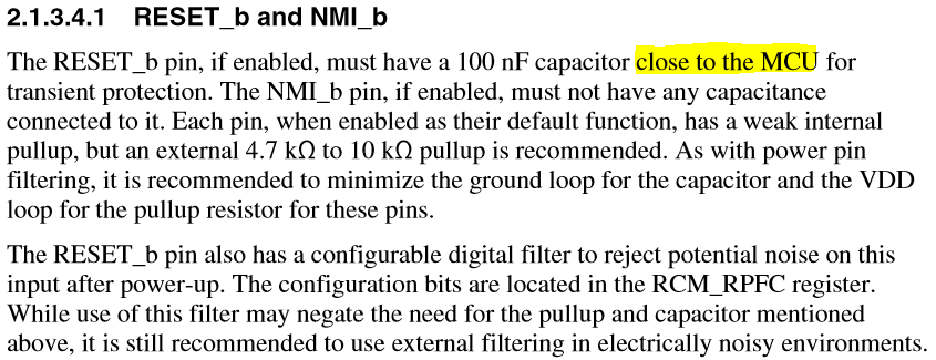
Please be sure that the cable is ~15 cm (or shorter). Also in the KQRUG, you can see that the NMI_b pin needs a pull up resistor and the RESET_b capacitor needs to be as closer to the MCU as possible.
Also, in the AN4835 in the section 3. Programming interfaces is mentioned that the EZP_CS pin (pin 9 in the 10-pin debug interface) must be in high to enable the SWD/JTAG functions. Please add a pull up resistor.
Best regards,
Earl.
- 新着としてマーク
- ブックマーク
- 購読
- ミュート
- RSS フィードを購読する
- ハイライト
- 印刷
- 不適切なコンテンツを報告
Hi,
I finally solved it. The schematic was wrong and the pin-out of the JTAG was not correct relative to the HW.
Regards,
Yulia


