- Forums
- Product Forums
- General Purpose MicrocontrollersGeneral Purpose Microcontrollers
- i.MX Forumsi.MX Forums
- QorIQ Processing PlatformsQorIQ Processing Platforms
- Identification and SecurityIdentification and Security
- Power ManagementPower Management
- Wireless ConnectivityWireless Connectivity
- RFID / NFCRFID / NFC
- Advanced AnalogAdvanced Analog
- MCX Microcontrollers
- S32G
- S32K
- S32V
- MPC5xxx
- Other NXP Products
- S12 / MagniV Microcontrollers
- Powertrain and Electrification Analog Drivers
- Sensors
- Vybrid Processors
- Digital Signal Controllers
- 8-bit Microcontrollers
- ColdFire/68K Microcontrollers and Processors
- PowerQUICC Processors
- OSBDM and TBDML
- S32M
- S32Z/E
-
- Solution Forums
- Software Forums
- MCUXpresso Software and ToolsMCUXpresso Software and Tools
- CodeWarriorCodeWarrior
- MQX Software SolutionsMQX Software Solutions
- Model-Based Design Toolbox (MBDT)Model-Based Design Toolbox (MBDT)
- FreeMASTER
- eIQ Machine Learning Software
- Embedded Software and Tools Clinic
- S32 SDK
- S32 Design Studio
- GUI Guider
- Zephyr Project
- Voice Technology
- Application Software Packs
- Secure Provisioning SDK (SPSDK)
- Processor Expert Software
- Generative AI & LLMs
-
- Topics
- Mobile Robotics - Drones and RoversMobile Robotics - Drones and Rovers
- NXP Training ContentNXP Training Content
- University ProgramsUniversity Programs
- Rapid IoT
- NXP Designs
- SafeAssure-Community
- OSS Security & Maintenance
- Using Our Community
-
- Cloud Lab Forums
-
- Knowledge Bases
- ARM Microcontrollers
- i.MX Processors
- Identification and Security
- Model-Based Design Toolbox (MBDT)
- QorIQ Processing Platforms
- S32 Automotive Processing Platform
- Wireless Connectivity
- CodeWarrior
- MCUXpresso Suite of Software and Tools
- MQX Software Solutions
- RFID / NFC
- Advanced Analog
-
- NXP Tech Blogs
- Home
- :
- 汎用マイクロコントローラ
- :
- Kinetisマイクロコントローラ
- :
- Interrupt latency time (cycles)
Interrupt latency time (cycles)
- RSS フィードを購読する
- トピックを新着としてマーク
- トピックを既読としてマーク
- このトピックを現在のユーザーにフロートします
- ブックマーク
- 購読
- ミュート
- 印刷用ページ
Interrupt latency time (cycles)
- 新着としてマーク
- ブックマーク
- 購読
- ミュート
- RSS フィードを購読する
- ハイライト
- 印刷
- 不適切なコンテンツを報告
Dear all
I'm checking the interrupt latency time of MK60DX256ZVLQ10.
The KQRUG is reporting:
"The NVIC is a standard module on the ARM Cortex M series. This module is closely
integrated with the core and provides a very low latency for entering an interrupt service
routine ISR (12 cycles) and exiting an ISR (12 cycles)."
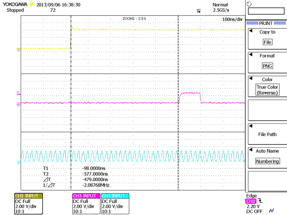
But, I'm observing a different behaviour. It is possible to check the wave below:
TRACE 1: the edge that generaete the interrupt (port E pin 0)
TRACE 2: a pin asserted immediately when ISR is started and deasserted at the end of ISR (port A pin 17)
TRACE 3: the TRACE_CLKOUT pin with system clock/2.
This is my simple ISR:
void PORTE_INT_HANDLER (void)
{
PORTE_ISFR |= 0x01;
GPIOA_PDOR |= 0x00020000;
GPIOA_PDOR &= ~0x00020000;
}
Can someone tell me why the latency is too big than 12 cycles?
thank you all..
Fabio
- 新着としてマーク
- ブックマーク
- 購読
- ミュート
- RSS フィードを購読する
- ハイライト
- 印刷
- 不適切なコンテンツを報告
Looking at the Kinetis K documentation, it looks to me that you will need to do the following to reduce interrupt latency as much as possible:
- Move the NVIC interrupt table to SRAM_L so that you will never incur a flash wait
- Also move your interrupt handler(s) to SRAM_L
You will probably want to split the handling into the low latency part in ram, and do the rest from flash. - Keep your stack, and data needed for the interrupt handler in SRAM_U
- Configure the crossbar switch for lowest latency for the hardware used by your handler(s).
For example, allow arbitration on undefined burst lengths, and park the peripheral bridge slave ports on the core system bus
It would also help to change your code to:
void PORTE_INT_HANDLER (void)
{
     // write directly to PSOR/PCOR instead of changing PDOR
     GPIOA_PSOR = 0x00020000;
     // ISFR is w1c, so just write the bits we want to clear
     PORTE_ISFR = 0x01;
     GPIOA_PCOR = 0x00020000;
}
- 新着としてマーク
- ブックマーク
- 購読
- ミュート
- RSS フィードを購読する
- ハイライト
- 印刷
- 不適切なコンテンツを報告
Fabio, your test is not measuring the interrupt latency. It is measuring the time from the application of the interrupt to the GPIO going high. You are forgetting to count the cycles generated by the entry overhead of the C ISR function and subsequent C bit setting statements.
There will be cycles used in the set up of the C interrupt function frame. There are at least 3 cycles used for PORTE_ISFR |= 0x01. One cycle to read PortE_ISFR to a register, one cycle to OR 0x01 into the register and a write of the register to PortE_ISFR. There are at least three cycles consumed in the setting of the output PIN. Notice how many cycles it takes for the signal to go from high to low with back to back C GPIO write statements in your example.
You need to look at the assembly code of the Interrupt function to find out how many cycles are being consumed before you set the GPIO pin. You need to subtract the cycles the C function used to get an accurate read of interrupt latency.
Norm
- 新着としてマーク
- ブックマーク
- 購読
- ミュート
- RSS フィードを購読する
- ハイライト
- 印刷
- 不適切なコンテンツを報告
Dear all,
thank you for the clarification, but i'm not underdtandig what is appening:
The instruction if ISR are:
0x00000000 PORTE_INT_HANDLER: cycles
0x00000000 0x01A0F24D movw r1,#53408 1
0x00000004 0x0104F2C4 movt r1,#16388 1
0x00000008 0x6808 ldr r0,[r1,#0] 2
0x0000000A 0x0001F040 orr r0,r0,#1 1
0x0000000E 0x6008 str r0,[r1,#0] 2
0x00000010 0x010CF24F movw r1,#61452 1
0x00000014 0x010FF2C4 movt r1,#16399 1
0x00000018 0x6808 ldr r0,[r1,#0] 2
0x0000001A 0x3000F440 orr r0,r0,#131072 1
0x0000001E 0x6008 str r0,[r1,#0] 2 tot= 14
0x00000020 0x010CF24F movw r1,#61452
0x00000024 0x010FF2C4 movt r1,#16399
0x00000028 0x6808 ldr r0,[r1,#0]
0x0000002A 0x3000F440 orr r0,r0,#131072
0x0000002E 0x6008 str r0,[r1,#0]
0x00000030 0x4770 bx lr
And if these calculations are right:
SYSTEM CLOCK 96,0E+6Hz --> T_CYCLE 10,4E-9 Sec
DELAYS CYCLES TIME (sec)
INTERRUPT LATECY 12 --> 125,0E-9
ISR INSTRUCTIONS EXECUTION 14 --> 145,8E-9
FLASH WAIT STATE@24MHz 41,7E-9
TOTAL 312,5E-9
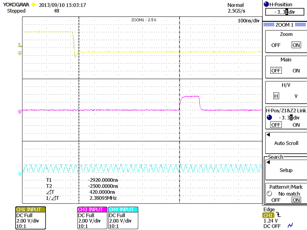
Why I'm measuring a delay of 420ns instead of 312?
- CH1 --> PTE0 interrupt enabled on falling edge.
- CH3 --> PTA17 toggle of pin done inside the ISR
- CH4 --> TRACE_CLKOUT
Where is my mistake? can someone help me?
Thank you
Fabio
- 新着としてマーク
- ブックマーク
- 購読
- ミュート
- RSS フィードを購読する
- ハイライト
- 印刷
- 不適切なコンテンツを報告
Hello Fabio,
When you are counting clock cycles in your code sequence you are only considering the time the core takes to execute the instruction.
In the MCU a write to a GPIO register traverses a Cross-bar switch and then a bus gasket and then it gets to the peripheral. If you assume best case being the core is not in contention on the crossbar for the GPIO slave bus( a good guess in this case) then the number of cycles through the cross bar is 1-2 cycles.
The number of clock cycles through the peripheral gasket into the peripheral is another 1-2 cycles. After the write completes in the core the actual write to the register could be 4 plus cycles later. The entire operation is going to take not 2 cycles but 6 cycles.
If you do a read from a peripheral the core is stalled for the 2-4 cycles while the read comes back with the result. Core execution may need to wait longer if the peripheral is in a different power domain. Peripherals like the LLWU, LPTMR, RTC, CMP, TSI are in a seperate power domain and syncronization between domains add addition cycles.
So that is why you are measuring 420 ns actually instead of the theoretical of 312. Because the theoretical is no accounting for the amount of time the core is waiting on the MCU read and writes to complete to the peripherals. The serialization of events in an embedded system is complicated by the inconsistency of the timing in the MCU. Add more complication if the core is not the only master on the cross-bar. The DMA could be enabled and could be arbitrating for the slave bus on the cross-bar, increasing the time the core is stalled awaiting the bus to be freed from the DMA.
I hope this helps.
Regards,
Philip
- 新着としてマーク
- ブックマーク
- 購読
- ミュート
- RSS フィードを購読する
- ハイライト
- 印刷
- 不適切なコンテンツを報告
Hi Philip
I'm trying to understand how to count cycles for ARM cortex M0+ processors to be able to predict the exact behavior. I would be happy for any comment.
I'm using FRDM-KL25Z board and Kinetis Studio.
I have a code is like this:
int main(void)
{
*/
SIM_SCGC5 |=0x400; //enable clock to port B
PORTB_PCR19 = 0x100; //Make PTB19 as GPIO
GPIOB_PDDR|=0x80000; //Make BTB19 as output pin
while(1)
{
GPIOB_PDOR &= ~0x80000; //turn green led on
GPIOB_PDOR |= 0x80000;
}
return 0;
}
Which compiles to (just the while loop):
while(1)
{
GPIOB_PDOR &= ~0x80000; //turn green led on <Baldur: set pin low>
548: 4b09 ldr r3, [pc, #36] ; (570 <main+0x54>) <Baldur: 2 cycles>
54a: 4a09 ldr r2, [pc, #36] ; (570 <main+0x54>) <Baldur: 2 cycles>
54c: 6811 ldr r1, [r2, #0] <Baldur: 2 cycles>
54e: 4a09 ldr r2, [pc, #36] ; (574 <main+0x58>) <Baldur: 2 cycles>
550: 400a ands r2, r1 <Baldur: 1 cycle>
552: 601a str r2, [r3, #0] <Baldur: 2 cycles>
C:\Users\baldurtho\workspace.kds\TestProject_005\Debug/../Sources/main.c:87 (discriminator 1)
GPIOB_PDOR |= 0x80000;
554: 4b06 ldr r3, [pc, #24] ; (570 <main+0x54>) <Baldur: 2 cycles>
556: 4a06 ldr r2, [pc, #24] ; (570 <main+0x54>) <Baldur: 2 cycles>
558: 6812 ldr r2, [r2, #0] <Baldur: 2 cycles>
55a: 2180 movs r1, #128 ; 0x80 <Baldur: 1 cycle>
55c: 0309 lsls r1, r1, #12 <Baldur: 1 cycle1>
55e: 430a orrs r2, r1 <Baldur: 1 cycle>
560: 601a str r2, [r3, #0] <Baldur: 2 cycles>
C:\Users\baldurtho\workspace.kds\TestProject_005\Debug/../Sources/main.c:90 (discriminator 1)
}
562: e7f1 b.n 548 <main+0x2c> <Baldur: 3 cycles>
564: 40047000 .word 0x40047000
568: 00001038 .word 0x00001038
56c: 4004a000 .word 0x4004a000
570: 400ff040 .word 0x400ff040
574: fff7ffff .word 0xfff7ffff
This code gave a square wave on the oscilloscope of 717 ns High and 618ns Low.
I counted instruction cycles and added to the above in <> brackets
(m0+ instruction set: http://infocenter.arm.com/help/index.jsp?topic=/com.arm.doc.ddi0432c/index.html)
To check my clock period I added 10 „nop“s and found it to be about 47.7ns.
So from the code without nops the 717ns is equavilent to 15 cycles and 618 is equavilent to 13 cycles
Low period: Counting cycles from line 552 (pin set low) to line 560 (pin set high) í count (my comments in the <> prackets) 11 cycles when scope said 13.
High period: counting cycles from line 560 to 552 i find 14 cycles but scope says 15
I have read that the m0+ processor has a 2 stage pipeline. Due to it I thought maybe the four 2 cycle instructions in row at line 548 to 54e would actually execute on every cycle and thus my actual program would be faster than the cycles for each instruction. But what I experience is the opposite, my code is slower than predicted.
I did some experiments and found that putting in one "ldr r3, [pc, #36]" instruction (inline assembly) to the c-code prolonged the time by time comparable to two cycles and adding two "ldr r3, [pc, #36]" in a row added four cycles. Could it be that the cycle count is given taking into account the two stage pipeline and expecting linear execution?
The Freescale Kinetis processors are said to have no wait states so that should not cause the slow down.
I was not able to test the length of all the instructions on my assembly output due to a strange problem: when I put in to my c-code the following: "__asm("orrs r2,r1"); I got the message that this instruction was not supported in Thumb16 mode - but I can see the instruction in my assembly above???
When I saw your post I realized that the time difference from my cycle counting to the output measured could be due to bus access. Do you think that could be the case here?
Again, I would be very happy for any comment.
Best regards,
Baldur
- 新着としてマーク
- ブックマーク
- 購読
- ミュート
- RSS フィードを購読する
- ハイライト
- 印刷
- 不適切なコンテンツを報告
In the last trace, the signal you see is the core clk which is the maximum speed while the NVIC module runs at the bus clk frequency [half the core speed], This is the reason you are observing 24 clk cycles between the interruption trigger and the interruption response.
- 新着としてマーク
- ブックマーク
- 購読
- ミュート
- RSS フィードを購読する
- ハイライト
- 印刷
- 不適切なコンテンツを報告
Dear Andrea,
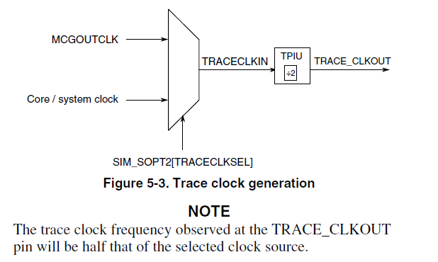
the last trace is the TRACE_CLKOUT, it is the half of clock source. As you can see here.
And the NVIC run at System clock not at Bus clock...
There is someone that can help me to undertand why the latency is too big than 12 cycles?
Thank you
Fabio


