- Forums
- Product Forums
- General Purpose MicrocontrollersGeneral Purpose Microcontrollers
- i.MX Forumsi.MX Forums
- QorIQ Processing PlatformsQorIQ Processing Platforms
- Identification and SecurityIdentification and Security
- Power ManagementPower Management
- Wireless ConnectivityWireless Connectivity
- RFID / NFCRFID / NFC
- Advanced AnalogAdvanced Analog
- MCX Microcontrollers
- S32G
- S32K
- S32V
- MPC5xxx
- Other NXP Products
- S12 / MagniV Microcontrollers
- Powertrain and Electrification Analog Drivers
- Sensors
- Vybrid Processors
- Digital Signal Controllers
- 8-bit Microcontrollers
- ColdFire/68K Microcontrollers and Processors
- PowerQUICC Processors
- OSBDM and TBDML
- S32M
- S32Z/E
-
- Solution Forums
- Software Forums
- MCUXpresso Software and ToolsMCUXpresso Software and Tools
- CodeWarriorCodeWarrior
- MQX Software SolutionsMQX Software Solutions
- Model-Based Design Toolbox (MBDT)Model-Based Design Toolbox (MBDT)
- FreeMASTER
- eIQ Machine Learning Software
- Embedded Software and Tools Clinic
- S32 SDK
- S32 Design Studio
- GUI Guider
- Zephyr Project
- Voice Technology
- Application Software Packs
- Secure Provisioning SDK (SPSDK)
- Processor Expert Software
- Generative AI & LLMs
-
- Topics
- Mobile Robotics - Drones and RoversMobile Robotics - Drones and Rovers
- NXP Training ContentNXP Training Content
- University ProgramsUniversity Programs
- Rapid IoT
- NXP Designs
- SafeAssure-Community
- OSS Security & Maintenance
- Using Our Community
-
- Cloud Lab Forums
-
- Knowledge Bases
- ARM Microcontrollers
- i.MX Processors
- Identification and Security
- Model-Based Design Toolbox (MBDT)
- QorIQ Processing Platforms
- S32 Automotive Processing Platform
- Wireless Connectivity
- CodeWarrior
- MCUXpresso Suite of Software and Tools
- MQX Software Solutions
- RFID / NFC
- Advanced Analog
-
- NXP Tech Blogs
- Home
- :
- 通用微控制器
- :
- Kinetis微控制器
- :
- Re: I2C configuration difference between MK10 and MK26
I2C configuration difference between MK10 and MK26
Hi,
I have mentioned a strange behavior of the I2C module in MK26 derivates (MK26FN2M0VLQ18).
Last year, I have mainly used MK10DX128VLH7 and MK20DX128VLH7 Kinetis derivates. I could reuse the same I2C software for configuration / send / transmit functions in almost every project.
Now, I try to initialize the I2C module in the Kinetis MK26FN2M0VLQ18 derivate without any success. I'm not sure where the problem is based on. In my opinion there isn't any difference between the datasheets.
NOTE:
A hardware problem can be excluded because:
1. I used a working I2C slave (BMP085 / Bosch) for my new project when I mentioned that there is a problem.
2. I used the following pull-up resistors for scl and sda: 1 kOhm, 3k3, 4k7 and 10 k without any success.
3. The electronic lead is shorter than 5 cm.
4. I tried clock frequencies between 30 kHz and 100 kHz. (Max. slave frequency 100 kHz)
5. The clock signal is how expected and the slew rate is excellent.
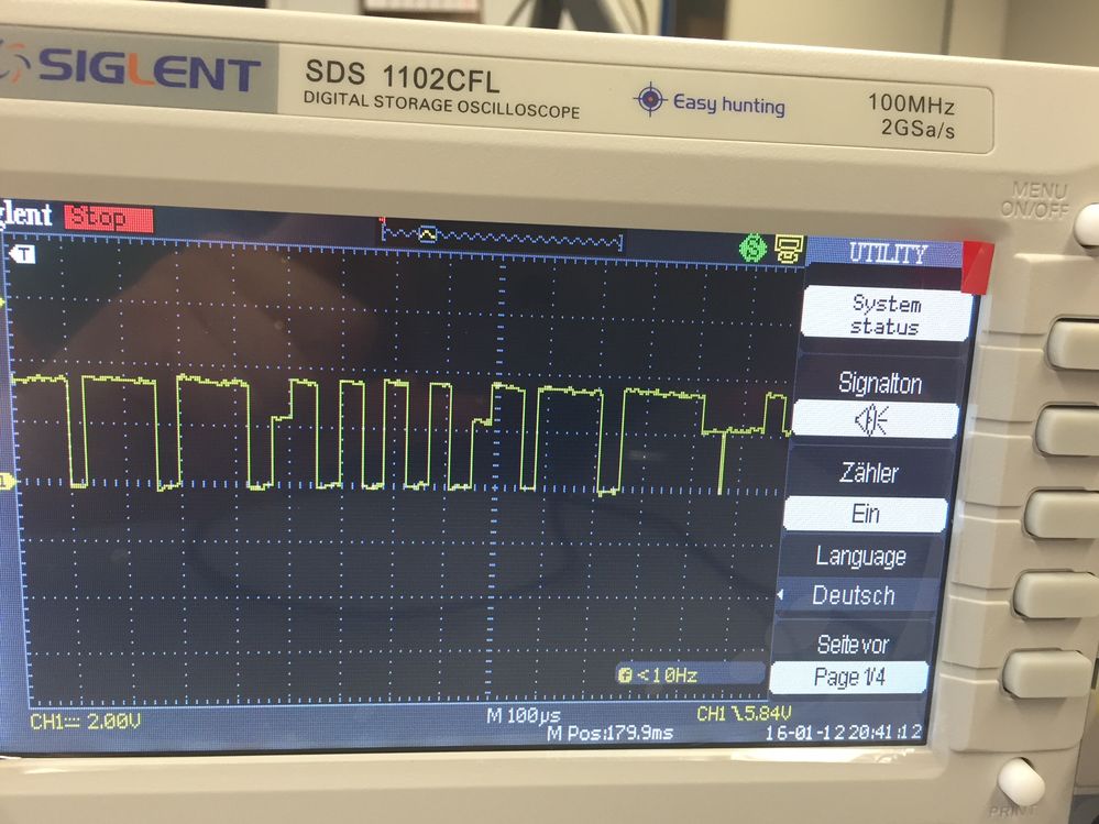
The picture below underlines my problem. I get middle voltage level when I suggest the acknowledge bit. So my slave isn't able to pull down the voltage level. (Independent of the pull-up resistor)
This missing acknowledge bit prohibit that I get the "receive acknowledge flag" and my conversation is not completed.
I tried to figure out why my (working) slave isn't able to pull down the voltage level. To get these information, I added a series resistor (1 kOhm) between the uC (sda) port and the slave (sda) port. Now, I can see two different sda signals. On the uC side, I see the sda signal without an acknowledge and on the slave side, I see the sda signal with an acknowledge (the middle voltage level are disappeared). So I can say, that there is a problem in my uC / or software.
To abbreviate I just post the first lines of code untill I get the error:
//Enable I2C0 clock
SIM_SCGC4 |= SIM_SCGC4_I2C0_MASK;
//Set Port B0 and B1 to ALT 2 (I2C0 / scl, sda)
PIN_CONFIG(B,0,_ALT2_);
PIN_CONFIG(B,1,_ALT2_);
//Initialize the I2C0 clock to 100kHz (60 MHz bus clock)
I2C0_F = 0x00
| I2C_F_ICR(0x2D)
| I2C_F_MULT(0x00);
//Enable the I2C0 module
I2C0_C1 = 0x00
| I2C_C1_IIEN_MASK;
//I2C start and master mode
//Busy?
while(I2C0_S & I2C_S_BUSY_MASK);
I2C0_C1 |= I2C_C1_TX_MASK
| I2C_C1_MST_MASK;
//I2C transmit
//Send device address (write): 0xEE
I2C0_D = 0xEE;
//Wait for transmission complete
//Transmission complete?
while(!(I2C0_S & I2C_S_TCF_MASK));
//Interrupt flag?
while(!(I2C0_S & I2C_S_IICIF_MAKS));
//Wait for the receive acknowledge flag!
//This flag is never set, because of the middle voltage levels!!!
while(I2C0_S & I2C_S_RXAK_MASK);
Can anyone help me with this problem? Or has anyone tried out the MK26FN2M0VLQ18 processor?
Thanks,
Pascal
已解决! 转到解答。
Hello Pascal Schroeer:
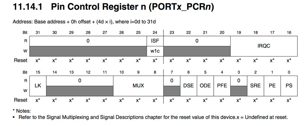
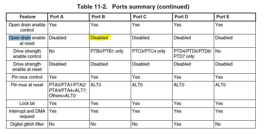
Have you configured the pins as Open-Drain? That is required for the I2C pins to operate as expected.
I guess this is the same issue as this thread: Can't have SDA completely low at ACK on HAL I2C ,MKV31
Regards!,
Jorge Gonzalez
-----------------------------------------------------------------------------------------------------------------------
Note: If this post answers your question, please click the Correct Answer button. Thank you!
-----------------------------------------------------------------------------------------------------------------------
Pascal
Apart form a few parts that have true open drain on the I2C it is alway necessary to configure the OD properties. This means that you must have done it with K10 and K20 parts in the past.
Regards
Mark
Hello Pascal Schroeer:
Have you configured the pins as Open-Drain? That is required for the I2C pins to operate as expected.
I guess this is the same issue as this thread: Can't have SDA completely low at ACK on HAL I2C ,MKV31
Regards!,
Jorge Gonzalez
-----------------------------------------------------------------------------------------------------------------------
Note: If this post answers your question, please click the Correct Answer button. Thank you!
-----------------------------------------------------------------------------------------------------------------------


