- Forums
- Product Forums
- General Purpose MicrocontrollersGeneral Purpose Microcontrollers
- i.MX Forumsi.MX Forums
- QorIQ Processing PlatformsQorIQ Processing Platforms
- Identification and SecurityIdentification and Security
- Power ManagementPower Management
- MCX Microcontrollers
- S32G
- S32K
- S32V
- MPC5xxx
- Other NXP Products
- Wireless Connectivity
- S12 / MagniV Microcontrollers
- Powertrain and Electrification Analog Drivers
- Sensors
- Vybrid Processors
- Digital Signal Controllers
- 8-bit Microcontrollers
- ColdFire/68K Microcontrollers and Processors
- PowerQUICC Processors
- OSBDM and TBDML
- S32M
-
- Solution Forums
- Software Forums
- MCUXpresso Software and ToolsMCUXpresso Software and Tools
- CodeWarriorCodeWarrior
- MQX Software SolutionsMQX Software Solutions
- Model-Based Design Toolbox (MBDT)Model-Based Design Toolbox (MBDT)
- FreeMASTER
- eIQ Machine Learning Software
- Embedded Software and Tools Clinic
- S32 SDK
- S32 Design Studio
- GUI Guider
- Zephyr Project
- Voice Technology
- Application Software Packs
- Secure Provisioning SDK (SPSDK)
- Processor Expert Software
- MCUXpresso Training Hub
-
- Topics
- Mobile Robotics - Drones and RoversMobile Robotics - Drones and Rovers
- NXP Training ContentNXP Training Content
- University ProgramsUniversity Programs
- Rapid IoT
- NXP Designs
- SafeAssure-Community
- OSS Security & Maintenance
- Using Our Community
-
- Cloud Lab Forums
-
- Knowledge Bases
- ARM Microcontrollers
- i.MX Processors
- Identification and Security
- Model-Based Design Toolbox (MBDT)
- QorIQ Processing Platforms
- S32 Automotive Processing Platform
- Wireless Connectivity
- CodeWarrior
- MCUXpresso Suite of Software and Tools
- MQX Software Solutions
-
- Home
- :
- 通用微控制器
- :
- Kinetis微控制器
- :
- Re: DDR2 setup time (tDS)/hold time (tDH) for DQ referring to data strobe (DQS) during read operation
DDR2 setup time (tDS)/hold time (tDH) for DQ referring to data strobe (DQS) during read operation
DDR2 setup time (tDS)/hold time (tDH) for DQ referring to data strobe (DQS) during read operation
Hi all,
I am running the DDR2 batch simulation. Before starting the simulation, I have developed the memory controller timing model (MCU model: MK61FN1M0VMJ15) through DDR2 controller timing model wizard. To develop the timing model, I need to get the setup time (tDS) and hold time (tDH) during the read operation.
Question 1
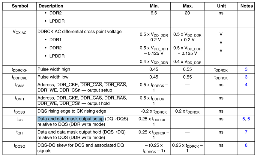
By refering to the datasheet of K61 MCU (Document Number: K61P256M150SF3) page 44. The datasheet only mention about the tQS and tQH during DDR write operation but didnt mention about the tDS and tDH for read operation. Do you guys know where to get this information ?
Question 2
When I read through the app note (AN10706) which is the document on developing the timing model for Hyperlynx simulation, I saw some of the memory controllers will delay the DQS by having 90 degree phase shift in their internal register. Not sure will the memory controller internal register will do the same thing during read operation? If yes, the datasheet didnt mention about the DQS skew during read operation in internal register. Do you guys know about this and where to get this information?
The following are the configuration for the memory controller,
DDR class: DDR2
Clock rate: 150 MHz
Regards,
SY Chan
Hi Jing Pan,
Thanks for your response.
AN10706 is an app note which discussed on how to create HyperLynx DDRx Memory Controller Timing Model. You may take a look on this document at following link,
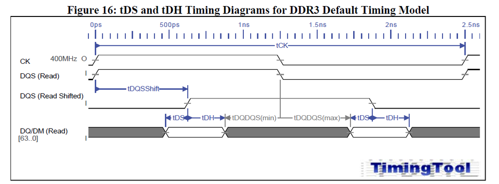
I understand that the DDR_DQ input signal is synchronous with DDR_DQS input signal and the DQ signal is edge aligned with the DQS signal. However, in order for the internal register of the memory controller to capture the input DDR_DQ signal correctly, the DDR_DQ signal must obey the setup time (tDS) and hold time (tDH) in reference with DQS signal. You may refer the following diagram for the tDS and tDH that used inside the AN10706 document.
The incoming DQ signal will have a phase shift of 90 degree when the internal register of the memory controller read the DQ signal which is one of my questions above (Not sure the internal register of the memory controller above will do a phase shift of 90 degree to the signal before reading). tDS and tDH refer to the setup and hold time that need to be fulfilled by the DQ signal in order for the internal register of the memory controller to read correctly.
Regards,
SY Chan
Hi Sing,
DQS is a bi-direct signal. In DDR read state, this signal send from SDRAM. DDR_D synchronous with DDR_DQS input. DQS edge aligned with data. There isn't tQS in reading. Config DDR interface is a very hard job. NXP has a config tool to simplify this work. Please get from https://www.nxp.com/downloads/en/initialization-boot-device-driver-code-generation/KINETIS_K70_DDR_I...
K70 and K61 has same die. You can use this tool on K61.
AN10706 is about hadling bare die. Do you mean any other doucment?
Regards,
Jing

