- Forums
- Product Forums
- General Purpose MicrocontrollersGeneral Purpose Microcontrollers
- i.MX Forumsi.MX Forums
- QorIQ Processing PlatformsQorIQ Processing Platforms
- Identification and SecurityIdentification and Security
- Power ManagementPower Management
- MCX Microcontrollers
- S32G
- S32K
- S32V
- MPC5xxx
- Other NXP Products
- Wireless Connectivity
- S12 / MagniV Microcontrollers
- Powertrain and Electrification Analog Drivers
- Sensors
- Vybrid Processors
- Digital Signal Controllers
- 8-bit Microcontrollers
- ColdFire/68K Microcontrollers and Processors
- PowerQUICC Processors
- OSBDM and TBDML
- S32M
-
- Solution Forums
- Software Forums
- MCUXpresso Software and ToolsMCUXpresso Software and Tools
- CodeWarriorCodeWarrior
- MQX Software SolutionsMQX Software Solutions
- Model-Based Design Toolbox (MBDT)Model-Based Design Toolbox (MBDT)
- FreeMASTER
- eIQ Machine Learning Software
- Embedded Software and Tools Clinic
- S32 SDK
- S32 Design Studio
- GUI Guider
- Zephyr Project
- Voice Technology
- Application Software Packs
- Secure Provisioning SDK (SPSDK)
- Processor Expert Software
- MCUXpresso Training Hub
-
- Topics
- Mobile Robotics - Drones and RoversMobile Robotics - Drones and Rovers
- NXP Training ContentNXP Training Content
- University ProgramsUniversity Programs
- Rapid IoT
- NXP Designs
- SafeAssure-Community
- OSS Security & Maintenance
- Using Our Community
-
- Cloud Lab Forums
-
- Knowledge Bases
- ARM Microcontrollers
- i.MX Processors
- Identification and Security
- Model-Based Design Toolbox (MBDT)
- QorIQ Processing Platforms
- S32 Automotive Processing Platform
- Wireless Connectivity
- CodeWarrior
- MCUXpresso Suite of Software and Tools
- MQX Software Solutions
-
- Home
- :
- i.MX Forums
- :
- i.MX RT Crossover MCUs
- :
- i.MXRT1064 FlexSPI: How to drive an external DSPI SRAM device
i.MXRT1064 FlexSPI: How to drive an external DSPI SRAM device
- Subscribe to RSS Feed
- Mark Topic as New
- Mark Topic as Read
- Float this Topic for Current User
- Bookmark
- Subscribe
- Mute
- Printer Friendly Page
i.MXRT1064 FlexSPI: How to drive an external DSPI SRAM device
- Mark as New
- Bookmark
- Subscribe
- Mute
- Subscribe to RSS Feed
- Permalink
- Report Inappropriate Content
On my custom board I have an SPI SRAM device ((e.g.: N01S830) connected to channel A of the FlexSPI peripheral on i.MXRT1064.
My target is to drive the SRAM device in Dual-SPI (DSPI) mode for data storage. But all of the SDK FlexSPI examples and all application documents refer to flash memory devices, mainly for boot code storage.
I started with SDK flexspi_nor_polling_transfer example, which operates on the external NOR flash memory mounted on the MIMXRT1064_EVK, but I cannot undestand how to interface and operate on a different SPI memory device.
To my SPI SRAM device I should set 20MHz maximum SPI clock frequency and send the following commands:
- Enable DUAL I/O access (command (1 byte)).
- Read data in burst mode starting at selected address (command (1 byte)+ address (3 bytes) + data (N bytes)).
- Write data in burst mode starting at selected address (command (1 byte) + address (3 bytes) + data (N bytes)).
Is there a step-by-step guide for setup and build a DSPI or QSPI interface to an external memory device with the FlexSPI peripheral?
Can I map my external SRAM in the i.MXRT1064 memory space (0x60000000) through the FlexSPI like external flash devices?
- Mark as New
- Bookmark
- Subscribe
- Mute
- Subscribe to RSS Feed
- Permalink
- Report Inappropriate Content
Hi @Vagni ,
There isn't a step by step guide for how to configure FlexSPI. Yes, you can start from the NOR flash example. You can also refer to RT685 pSRAM example. But it is a 8-bit pSRAM.
Yes, you can put SRAM in 0x60000000.
Regards,
Jing
- Mark as New
- Bookmark
- Subscribe
- Mute
- Subscribe to RSS Feed
- Permalink
- Report Inappropriate Content
Hi Jing, thanks for your reply.
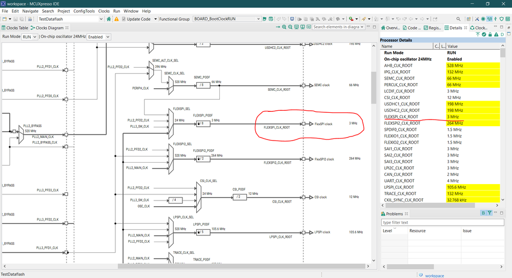
My custom board is based on the MIMXRT1064CVL5A mcu. I use the on-chip 24MHz oscillator to directly feed PLL3_PFD0_CLK (bypassing PLL3_PFD0), which I select as FlexSPI source clock with prescaler 8 (FLEXSPI_PODF) in order to get 3 MHz as FLEXSPI_CLK_ROOT. This should be the SCLK clock driving the esternal serial SRAM in SDR mode, right?

I setup my LUT for the serial SRAM. The following is the flexspi_device_config_t structure I use when I call FLEXSPI_SetFlashConfig() driver function (my target is to map the serial SRAM in memory, accessing to it in DSPI mode):
static const flexspi_device_config_t deviceconfig =
{
    .flexspiRootClk       = 3000000,								/*!< FLEXSPI serial root clock (<20 MHz) */
	.isSck2Enabled        = 0,										/*!< FLEXSPI use SCK2. */
    .flashSize            = SRAM_SIZE,								/*!< memory size in KByte. */
    .CSIntervalUnit       = kFLEXSPI_CsIntervalUnit1SckCycle,		/*!< CS interval unit, 1 or 256 serial root clock cycle. */
    .CSInterval           = 1,										/*!< CS line assert interval, multiply CS interval unit to
                                                      	  	  	  	  	 get the CS line assert interval cycles (> 25ns) */
    .CSHoldTime           = 1,										/*!< CS line hold time (> 50ns) */
    .CSSetupTime          = 1,										/*!< CS line setup time (> 25ns) */
    .dataValidTime        = 0,										/*!< Data valid time for external device. */
    .columnspace          = 0,										/*!< Column space size. */
    .enableWordAddress    = 0,										/*!< If enable word address.*/
    .AWRSeqIndex          = SRAM_CMD_LUT_SEQ_IDX_WRITE_DUAL,		/*!< Sequence ID for AHB write command. */
    .AWRSeqNumber         = 1,										/*!< Sequence number for AHB write command. */
    .ARDSeqIndex          = SRAM_CMD_LUT_SEQ_IDX_READ_DUAL,			/*!< Sequence ID for AHB read command. */
    .ARDSeqNumber         = 1,										/*!< Sequence number for AHB read command. */
    .AHBWriteWaitUnit     = kFLEXSPI_AhbWriteWaitUnit2AhbCycle,		/*!< AHB write wait unit. */
    .AHBWriteWaitInterval = 0,										/*!< AHB write wait interval, multiply AHB write interval
                                                      	  	  	  	  unit to get the AHB write wait cycles. */
	.enableWriteMask      = 0,										/*!< Enable/Disable FLEXSPI drive DQS pin as write mask
                                                      	  	  	  	  when writing to external device. */
};
Before I initialize FlexSPI with the following flexspi_config_t structure:
    /*Set AHB buffer size for reading data through AHB bus. */
    config.ahbConfig.enableAHBPrefetch    = true;
    config.ahbConfig.enableAHBBufferable  = true;
    config.ahbConfig.enableReadAddressOpt = true;
    config.ahbConfig.enableAHBCachable    = true;
    config.rxSampleClock                  = kFLEXSPI_ReadSampleClkLoopbackInternally;
    FLEXSPI_Init(base, &config);
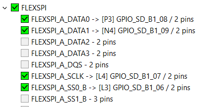
On my board no FlexSPI DQS pin is available (the two possible pins are all used as GPIO):

Then I try to read (in normal SPI mode) the 1-byte SRAM Mode Register with the following function (2-byte SPI transaction: command byte + data byte):
status_t flexspi_sram_get_mode(FLEXSPI_Type *base, uint8_t *mode)
{
    uint32_t temp = 0xFFFFFFFFUL;
    flexspi_transfer_t flashXfer;

    flashXfer.deviceAddress = 0;
    flashXfer.port          = kFLEXSPI_PortA1;
    flashXfer.cmdType       = kFLEXSPI_Read;
    flashXfer.SeqNumber     = 1;
    flashXfer.seqIndex      = SRAM_CMD_LUT_SEQ_IDX_RDMR;
    flashXfer.data          = &temp;
    flashXfer.dataSize      = 1;

    status_t status = FLEXSPI_TransferBlocking(base, &flashXfer);

    *mode = temp;

    /* Do software reset or clear AHB buffer directly. */
#if defined(FSL_FEATURE_SOC_OTFAD_COUNT) && defined(FLEXSPI_AHBCR_CLRAHBRXBUF_MASK) && \
    defined(FLEXSPI_AHBCR_CLRAHBTXBUF_MASK)
    base->AHBCR |= FLEXSPI_AHBCR_CLRAHBRXBUF_MASK | FLEXSPI_AHBCR_CLRAHBTXBUF_MASK;
    base->AHBCR &= ~(FLEXSPI_AHBCR_CLRAHBRXBUF_MASK | FLEXSPI_AHBCR_CLRAHBTXBUF_MASK);
#else
    FLEXSPI_SoftwareReset(base);
#endif

    return status;
}
I see my function exits with success, but FlexSPI peripheral actives SRAM chip-select (FLEXSPI_A_SS0_B) for about 200 ns and output 16 clock cycles at about 100 MHz. Obviously, what I read is nonsense, because SRAM maximum SPI clock is 20 MHz.
Where does that 100 MHz clock come from? Can you help me to achieve a right SCLK clock frequency?
- Mark as New
- Bookmark
- Subscribe
- Mute
- Subscribe to RSS Feed
- Permalink
- Report Inappropriate Content
Hi @Vagni ,
Please check if you have update code after change in clock config tool. And in flexspi_nor_flash_init(), there is a flexspi_clock_init(). Have you disabled it?
Regards,
Jing
- Mark as New
- Bookmark
- Subscribe
- Mute
- Subscribe to RSS Feed
- Permalink
- Report Inappropriate Content
Yes, the clock_config code is updated:
#define BOARD_BOOTCLOCKRUN_FLEXSPI_CLK_ROOT 3000000ULAlso, in my flexspi_sram_init() the flexspi_clock_init() call is remarked.
- Mark as New
- Bookmark
- Subscribe
- Mute
- Subscribe to RSS Feed
- Permalink
- Report Inappropriate Content
Hi @Vagni ,
You can read back related register to check the real frequency.
static inline uint32_t flexspi_get_frequency(void)
{
uint32_t div;
uint32_t fre;
/* Clock divider:
000 divided by 1
001 divided by 2
010 divided by 3
011 divided by 4
100 divided by 5
101 divided by 6
110 divided by 7
111 divided by 8
*/
div = CLOCK_GetDiv(kCLOCK_FlexspiDiv);
/* Get frequency */
fre = CLOCK_GetFreq(kCLOCK_Usb1PllPfd0Clk) / (div + 0x01U);
return fre;
}
Regards,
Jing
- Mark as New
- Bookmark
- Subscribe
- Mute
- Subscribe to RSS Feed
- Permalink
- Report Inappropriate Content
And the returned real frequency is 90000000 (90 MHz)!
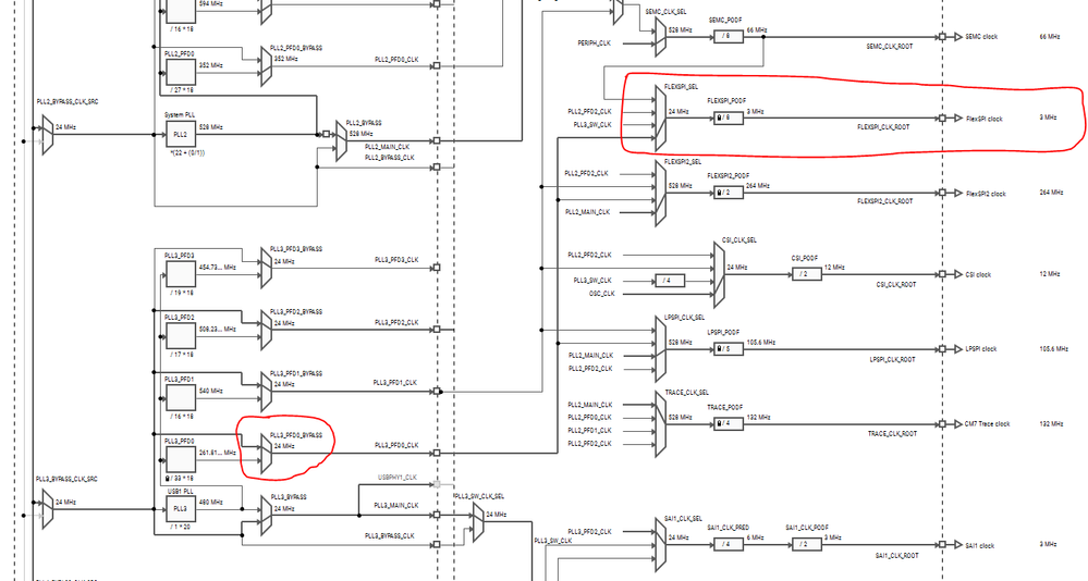
I don't understand how is possible.... The following is my clocks diagram in the clock configuration tool:

Attached are my clock_config source files. I cannot see my PLL3_PFD0_BYPASS setting in these files, in order to bypass PLL3_PFD0 and have PLL3_PFD0_CLK = 24 MHz to be selected with FLEXSPI_SEL mux as FlexSPI source clock (then divided per 8 with FLESPI_PODF).
In my main() function I call BORAD_InitBootClocks(), which should set clocks with that configuration.
/*!
 * @brief Main function
 */
int main(void)
{
    BOARD_ConfigMPU();
    /* Board pin init */
    BOARD_InitBootPins();
    BOARD_InitBootClocks();
    /* Update the core clock */
    SystemCoreClockUpdate();

    BOARD_InitDebugConsole();

[...]

}
Where am I wrong?
- Mark as New
- Bookmark
- Subscribe
- Mute
- Subscribe to RSS Feed
- Permalink
- Report Inappropriate Content
Hi ,
You can trace it step by step.
Regards,
Jing
- Mark as New
- Bookmark
- Subscribe
- Mute
- Subscribe to RSS Feed
- Permalink
- Report Inappropriate Content
Hi Jing,
I realized every change I make on PLL3 (USB1 PLL) in Clock Configuration Tool is useless when the macro XIP_EXTERNAL_FLASH is defined, as it is in my project.
    /* In SDK projects, external flash (configured by FLEXSPI2) will be initialized by dcd.
     * With this macro XIP_EXTERNAL_FLASH, usb1 pll (selected to be FLEXSPI2 clock source in SDK projects) will be left unchanged.
     * Note: If another clock source is selected for FLEXSPI2, user may want to avoid changing that clock as well.*/
#if !(defined(XIP_EXTERNAL_FLASH) && (XIP_EXTERNAL_FLASH == 1))
    /* Init Usb1 PLL. */
    CLOCK_InitUsb1Pll(&usb1PllConfig_BOARD_BootClockRUN);
    /* Init Usb1 pfd0. */
    CLOCK_InitUsb1Pfd(kCLOCK_Pfd0, 33);
    /* Init Usb1 pfd1. */
    CLOCK_InitUsb1Pfd(kCLOCK_Pfd1, 16);
    /* Init Usb1 pfd2. */
    CLOCK_InitUsb1Pfd(kCLOCK_Pfd2, 17);
    /* Init Usb1 pfd3. */
    CLOCK_InitUsb1Pfd(kCLOCK_Pfd3, 19);
    /* Disable Usb1 PLL output for USBPHY1. */
    CCM_ANALOG->PLL_USB1 &= ~CCM_ANALOG_PLL_USB1_EN_USB_CLKS_MASK;
#endif
Since PLL3 is used to drive FlexSPI2 interface to the internal flash memory, every change I make on PLL3 is always generated within the #if/#endif construct above, so it is excluded in the build process.
Where can I find how PLL3 is configured, in order to know the actual PLL3 clocks values?
My application has to use SDRAM and USDHC, so I cannot use neither SEMC_CLK_ROOT clock nor PLL2_PFD2_CLK clock to drive the FlexSPI (they would be too much high).
So, only high clock devices can be driven with FlexSPI? How can I generate a FLEXSPI_CLK_ROOT clock not greater then 20MHz?
- Mark as New
- Bookmark
- Subscribe
- Mute
- Subscribe to RSS Feed
- Permalink
- Report Inappropriate Content
Hi @Vagni ,
I looked it over. Yes, it seems you can't use this PSRAM. It's too slow. None of the clock source can give such a low speed clock. But there are many high speed PSRAM you can use.
Regards,
Jing
- Mark as New
- Bookmark
- Subscribe
- Mute
- Subscribe to RSS Feed
- Permalink
- Report Inappropriate Content
Hi Jing,
Thank you for your reply. I just have three question:
- Where is the FlexSPI2 clock initialization in a i.MXRT1064 project? Maybe in the XIP source files? Or among eFuses (on my board I don't use GPIO boot overrides)? Or in the DCD source files? Till now, I don't understand how XIP and DCD source files work in my project (coming from flexspi_nor_polling_transfer sample project).
- When I try to execute my code step-by-step with debugger (P&E Multilink connected on SWD), in flexSPI functions the debugger is always suddenly disconnected; and for recovery I need a power-cycle on my board. I don't understand why; may the cause be the CACHE_MAINTAIN = 1 macro?
- During my tests with different source clocks, in some cases the FLEXSPI_Init() is blocked waiting FlexSPI peripheral out of software reset: the SWRESET bit in the MCR0 register never auto-clears itself. What could be the cause?
- Mark as New
- Bookmark
- Subscribe
- Mute
- Subscribe to RSS Feed
- Permalink
- Report Inappropriate Content
Hi @Vagni ,
1. In the project, there is a structure called qspiflash_conifg which you can find in evkmimxrt1064_flexspi_nor_config.c. ROM bootloader will read this structure in a low speed. Then configure the SPI clock.
2. When MCU start to execute the code in FlexSPI, you'd better don't change the FlexSPI clock. If you have to change it, you can copy related code to SRAM and change clock by the code in SRAM. In the flexspi demo, CACHE_MAINTAIN is used to invalidate DCACHE. It should not cause debug disconnection.
3. That should means flexspi soft reset fail. Could it because the clock out of range?
Regards,
Jing