- Forums
- Product Forums
- General Purpose MicrocontrollersGeneral Purpose Microcontrollers
- i.MX Forumsi.MX Forums
- QorIQ Processing PlatformsQorIQ Processing Platforms
- Identification and SecurityIdentification and Security
- Power ManagementPower Management
- MCX Microcontrollers
- S32G
- S32K
- S32V
- MPC5xxx
- Other NXP Products
- Wireless Connectivity
- S12 / MagniV Microcontrollers
- Powertrain and Electrification Analog Drivers
- Sensors
- Vybrid Processors
- Digital Signal Controllers
- 8-bit Microcontrollers
- ColdFire/68K Microcontrollers and Processors
- PowerQUICC Processors
- OSBDM and TBDML
- S32M
-
- Solution Forums
- Software Forums
- MCUXpresso Software and ToolsMCUXpresso Software and Tools
- CodeWarriorCodeWarrior
- MQX Software SolutionsMQX Software Solutions
- Model-Based Design Toolbox (MBDT)Model-Based Design Toolbox (MBDT)
- FreeMASTER
- eIQ Machine Learning Software
- Embedded Software and Tools Clinic
- S32 SDK
- S32 Design Studio
- GUI Guider
- Zephyr Project
- Voice Technology
- Application Software Packs
- Secure Provisioning SDK (SPSDK)
- Processor Expert Software
- MCUXpresso Training Hub
-
- Topics
- Mobile Robotics - Drones and RoversMobile Robotics - Drones and Rovers
- NXP Training ContentNXP Training Content
- University ProgramsUniversity Programs
- Rapid IoT
- NXP Designs
- SafeAssure-Community
- OSS Security & Maintenance
- Using Our Community
-
- Cloud Lab Forums
-
- Knowledge Bases
- ARM Microcontrollers
- i.MX Processors
- Identification and Security
- Model-Based Design Toolbox (MBDT)
- QorIQ Processing Platforms
- S32 Automotive Processing Platform
- Wireless Connectivity
- CodeWarrior
- MCUXpresso Suite of Software and Tools
- MQX Software Solutions
-
- Home
- :
- i.MX フォーラム
- :
- i.MXプロセッサ
- :
- iMX8MPlus: Does the MIPI-CSI interface require the low-speed signaling?
iMX8MPlus: Does the MIPI-CSI interface require the low-speed signaling?
- RSS フィードを購読する
- トピックを新着としてマーク
- トピックを既読としてマーク
- このトピックを現在のユーザーにフロートします
- ブックマーク
- 購読
- ミュート
- 印刷用ページ
- 新着としてマーク
- ブックマーク
- 購読
- ミュート
- RSS フィードを購読する
- ハイライト
- 印刷
- 不適切なコンテンツを報告
Hi,
Our customer E4D raised the following question:
Questions have arisen around whether we can just wire up the differential pairs for:
Clock Lane, Data Lane 0, Data Lane 1, Data Lane 2, Data Lane 3 directly to the i.mx8MPlus's 1st CSI port "CSI1",
or do we need to provide the low-speed signaling out of the FPGA also. That involves still involves only differential pairs
going into the i.mx8, but the FPGA has to provide extra output pins and termination to allow the extra pins to drive low-speed bi-directional
signaling.
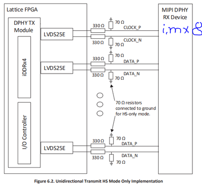
What raises the question is that Lattice shows multiple ways to wire up the part, one of which omits the LS (low-speed) signaling.
It would simplify our design, but we are unsure whether it would work, as most sources claim you need both HS and LS signaling support
for MIPI-CSI2 to work.
Can you confirm whether the i.mx8MPlus requires the low-speed signaling? And if not, how to configure the part to allow high-speed only?
For reference, this is the interfacing Lattice proposes for HS & LS signaling:
And this is the interfacing they propose for HS-only signaling:
Thanks.
Ayman
解決済! 解決策の投稿を見る。
- 新着としてマーク
- ブックマーク
- 購読
- ミュート
- RSS フィードを購読する
- ハイライト
- 印刷
- 不適切なコンテンツを報告
i.MX 8MP require the connected camera to work in the LP state before enabling the Rx DPHY. if only HS signal, the Dphy would couldn't detect the HS mode and wrongly set to the stop mode for ever
- 新着としてマーク
- ブックマーク
- 購読
- ミュート
- RSS フィードを購読する
- ハイライト
- 印刷
- 不適切なコンテンツを報告
i.MX 8MP require the connected camera to work in the LP state before enabling the Rx DPHY. if only HS signal, the Dphy would couldn't detect the HS mode and wrongly set to the stop mode for ever
- 新着としてマーク
- ブックマーク
- 購読
- ミュート
- RSS フィードを購読する
- ハイライト
- 印刷
- 不適切なコンテンツを報告
Thanks a lot.
Ayman

