- Forums
- Product Forums
- General Purpose MicrocontrollersGeneral Purpose Microcontrollers
- i.MX Forumsi.MX Forums
- QorIQ Processing PlatformsQorIQ Processing Platforms
- Identification and SecurityIdentification and Security
- Power ManagementPower Management
- Wireless ConnectivityWireless Connectivity
- RFID / NFCRFID / NFC
- MCX Microcontrollers
- S32G
- S32K
- S32V
- MPC5xxx
- Other NXP Products
- S12 / MagniV Microcontrollers
- Powertrain and Electrification Analog Drivers
- Sensors
- Vybrid Processors
- Digital Signal Controllers
- 8-bit Microcontrollers
- ColdFire/68K Microcontrollers and Processors
- PowerQUICC Processors
- OSBDM and TBDML
- S32M
-
- Solution Forums
- Software Forums
- MCUXpresso Software and ToolsMCUXpresso Software and Tools
- CodeWarriorCodeWarrior
- MQX Software SolutionsMQX Software Solutions
- Model-Based Design Toolbox (MBDT)Model-Based Design Toolbox (MBDT)
- FreeMASTER
- eIQ Machine Learning Software
- Embedded Software and Tools Clinic
- S32 SDK
- S32 Design Studio
- GUI Guider
- Zephyr Project
- Voice Technology
- Application Software Packs
- Secure Provisioning SDK (SPSDK)
- Processor Expert Software
-
- Topics
- Mobile Robotics - Drones and RoversMobile Robotics - Drones and Rovers
- NXP Training ContentNXP Training Content
- University ProgramsUniversity Programs
- Rapid IoT
- NXP Designs
- SafeAssure-Community
- OSS Security & Maintenance
- Using Our Community
-
- Cloud Lab Forums
-
- Knowledge Bases
- ARM Microcontrollers
- i.MX Processors
- Identification and Security
- Model-Based Design Toolbox (MBDT)
- QorIQ Processing Platforms
- S32 Automotive Processing Platform
- Wireless Connectivity
- CodeWarrior
- MCUXpresso Suite of Software and Tools
- MQX Software Solutions
-
- Home
- :
- i.MX Forums
- :
- i.MX Processors
- :
- Re: i.MX8MP DDR Bring Up MSCALE Tool
i.MX8MP DDR Bring Up MSCALE Tool
- Subscribe to RSS Feed
- Mark Topic as New
- Mark Topic as Read
- Float this Topic for Current User
- Bookmark
- Subscribe
- Mute
- Printer Friendly Page
- Mark as New
- Bookmark
- Subscribe
- Mute
- Subscribe to RSS Feed
- Permalink
- Report Inappropriate Content
Hello,
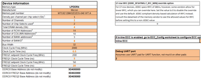
We are trying to bring up our custom board with i.MX8M-plus MPU. We have generated a script like below for our 512 MB LPDDR4 Ram from Micron, configuration is like below for the MT53E128M32D2DS-046 WT:A LPDDR4 Ram:
After generating script according to the configuration above, we get the following results from MSCALE tool:
Download is complete
Waiting for the target board boot...

===================hardware_init=====================


********Found PMIC PCA9450**********
hardware_init exit

*************************************************************************

*************************************************************************

*************************************************************************
       MX8 DDR Stress Test V3.30
       Built on Nov 24 2021 13:52:12
*************************************************************************

Waiting for board configuration from PC-end...

--Set up the MMU and enable I and D cache--
   - This is the Cortex-A53 core
  - Check if I cache is enabled
  - Enabling I cache since it was disabled
  - Push base address of TTB to TTBR0_EL3
  - Config TCR_EL3
  - Config MAIR_EL3
  - Enable MMU
  - Data Cache has been enabled
  - Check system memory register, only for debug

   - VMCR Check:
   - ttbr0_el3: 0x97d000
   - tcr_el3: 0x2051c
   - mair_el3: 0x774400
   - sctlr_el3: 0xc01815
   - id_aa64mmfr0_el1: 0x1122

  - MMU and cache setup complete

*************************************************************************
            ARM clock(CA53) rate: 1800MHz
            DDR Clock: 2000MHz

============================================
        DDR configuration
DDR type is LPDDR4
Data width: 32, bank num: 8
Row size: 14, col size: 10
Two chip selects are used
Number of DDR controllers used on the SoC: 1
Density per chip select:   512MB
Density per controller is: 1024MB
Total density detected on the board is: 1024MB
============================================

MX8M-plus: Cortex-A53 is found

*************************************************************************

============ Step 1: DDRPHY Training... ============
---DDR 1D-Training @2000Mhz...
PMU: Error: CA Training Failed.
PMU: ***** Assertion Error - terminating *****
[Result] FAILED
Why is Total Density Detected on the board LOG 1024MB when it should be 512MB, according to our configuration?
Solved! Go to Solution.
- Mark as New
- Bookmark
- Subscribe
- Mute
- Subscribe to RSS Feed
- Permalink
- Report Inappropriate Content
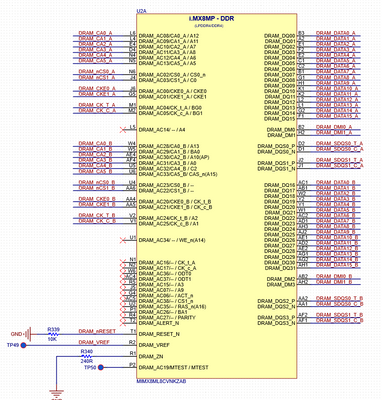
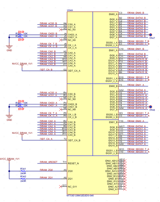
Hi @Wobaffet,
Thanks for sharing the schematic section.
Please refer to the LPDDR4 datasheet. The LPDDR4 used in the design has a Dual-Die, Dual-Channel, Single-Rank configuration. So, there are no CS1_A and CS1_B pins in the LPDDR4. If you see in the LPDDR4 datasheet, pins R3 and H3 are NC. So, there is no meaning in the connection to these pins.
Since this is the single rank configuration, only 1 chip select is required to be used. So, the number of chip selects used should be 1 in the RPA file and not 2.
I hope it helps!
Thanks & Regards,
Ritesh M Patel
- Mark as New
- Bookmark
- Subscribe
- Mute
- Subscribe to RSS Feed
- Permalink
- Report Inappropriate Content
Hello Ritesh,
Thank you for your response, I've attached the schematics. Also, how can we perform a stress test for our RAM @2Ghz.
- Mark as New
- Bookmark
- Subscribe
- Mute
- Subscribe to RSS Feed
- Permalink
- Report Inappropriate Content
Hi @Wobaffet,
Thanks for sharing the schematic section.
Please refer to the LPDDR4 datasheet. The LPDDR4 used in the design has a Dual-Die, Dual-Channel, Single-Rank configuration. So, there are no CS1_A and CS1_B pins in the LPDDR4. If you see in the LPDDR4 datasheet, pins R3 and H3 are NC. So, there is no meaning in the connection to these pins.
Since this is the single rank configuration, only 1 chip select is required to be used. So, the number of chip selects used should be 1 in the RPA file and not 2.
I hope it helps!
Thanks & Regards,
Ritesh M Patel
- Mark as New
- Bookmark
- Subscribe
- Mute
- Subscribe to RSS Feed
- Permalink
- Report Inappropriate Content
Hello Ritesh,
Thank you so much for the clarification.
We want to test our layout @2GHz, but I think MSCALE DDR stress test does not do this by default, how can we accomplish this?
We have tried to flash u-boot with MSCALE-generated binaries but we get the following log from Cortex A debug uart:
DDRINFO: start DRAM init
DDRINFO: DRAM rate 4000MTS
Training FAILED
Thank you in advance!
Best Regards.
- Mark as New
- Bookmark
- Subscribe
- Mute
- Subscribe to RSS Feed
- Permalink
- Report Inappropriate Content
Hi @Wobaffet,
Did you port the 'lpddr4_timing.c' file (generated after the successful stress test) to the u-boot?
Thanks & Regards,
Ritesh M Patel
- Mark as New
- Bookmark
- Subscribe
- Mute
- Subscribe to RSS Feed
- Permalink
- Report Inappropriate Content
Hello @riteshmpatel
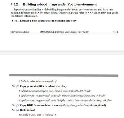
I followed the guide on the MSCALE_DDR_Tool_User_Guide.pdf, for yocto environment.
- Mark as New
- Bookmark
- Subscribe
- Mute
- Subscribe to RSS Feed
- Permalink
- Report Inappropriate Content
- Mark as New
- Bookmark
- Subscribe
- Mute
- Subscribe to RSS Feed
- Permalink
- Report Inappropriate Content
Hello @riteshmpatel,
For our board we have minimum configuration, we only configured emmc, ram, and usb as type B so we've made below patches. As for the timing, we have only followed MSCALE tool user guide. Our patches for the u-boot is attached.
The instructions from MSCALE guide:
- Mark as New
- Bookmark
- Subscribe
- Mute
- Subscribe to RSS Feed
- Permalink
- Report Inappropriate Content
Hello @riteshmpatel
We have an update, we were able to boot our board, I needed to do a clean build with the patches I've provided to you. I think when u-boot compiled alone with timing file did not applied somehow, I shared our log and I have few questions.
We've configured our emmc for the usdhc3, but on the log it shows it boots from emmc2.
Also is there any application or process to run more tests on the RAM to see if our layout is okay?
Thank you in advance!
Best Regards
- Mark as New
- Bookmark
- Subscribe
- Mute
- Subscribe to RSS Feed
- Permalink
- Report Inappropriate Content
Hi @Wobaffet,
Good to hear that.
The reason it shows eMMC2 is because the numbering starts from eMMC0.
If the Overnight Stress test runs successfully on the intended frequency range, then there shall be no issues with RAM.
Thanks & Regards,
Ritesh M Patel
- Mark as New
- Bookmark
- Subscribe
- Mute
- Subscribe to RSS Feed
- Permalink
- Report Inappropriate Content
Hello @riteshmpatel
Thank you for all the help.
by meaning overnight stress test runs, you mean the one on the MSCALE tool?
I'am using stress-ng for now, our RAM is 512MB, 450MB is seen by the os and 376MB free space available. So does testing RAM for only 300MB when board is up and running would be sufficient?
Or should I use MSCALE tool? If so what should be the start and end frequencies should be for our 2GHz Ram at the below screen shot?
Thank you in advance!
Best Regards.
- Mark as New
- Bookmark
- Subscribe
- Mute
- Subscribe to RSS Feed
- Permalink
- Report Inappropriate Content
When I changed the CS option on the RPA tool to 1 from 2, it worked, and the calibration, and stress test passed.
- Why did it work with CS 1?
- Does the MSCALE Tool DDR stress test, test the RAM on 2GHz?
Thank you in advance.
Best Regards!
- Mark as New
- Bookmark
- Subscribe
- Mute
- Subscribe to RSS Feed
- Permalink
- Report Inappropriate Content
Here is the LOG:
Download is complete
Waiting for the target board boot...

===================hardware_init=====================


********Found PMIC PCA9450**********
hardware_init exit

*************************************************************************

*************************************************************************

*************************************************************************
       MX8 DDR Stress Test V3.30
       Built on Nov 24 2021 13:52:12
*************************************************************************

Waiting for board configuration from PC-end...

--Set up the MMU and enable I and D cache--
   - This is the Cortex-A53 core
  - Check if I cache is enabled
  - Enabling I cache since it was disabled
  - Push base address of TTB to TTBR0_EL3
  - Config TCR_EL3
  - Config MAIR_EL3
  - Enable MMU
  - Data Cache has been enabled
  - Check system memory register, only for debug

   - VMCR Check:
   - ttbr0_el3: 0x97d000
   - tcr_el3: 0x2051c
   - mair_el3: 0x774400
   - sctlr_el3: 0xc01815
   - id_aa64mmfr0_el1: 0x1122

  - MMU and cache setup complete

*************************************************************************
            ARM clock(CA53) rate: 1800MHz
            DDR Clock: 2000MHz

============================================
        DDR configuration
DDR type is LPDDR4
Data width: 32, bank num: 8
Row size: 14, col size: 10
One chip select is used
Number of DDR controllers used on the SoC: 1
Density per chip select:   512MB
Density per controller is: 512MB
Total density detected on the board is: 512MB
============================================

MX8M-plus: Cortex-A53 is found

*************************************************************************

============ Step 1: DDRPHY Training... ============
---DDR 1D-Training @2000Mhz...
[Process] End of CA training
[Process] End of initialization
[Process] End of read enable training
[Process] End of fine write leveling
[Process] End of read DQ deskew training
[Process] End of MPR read delay center optimization
[Process] End of Write Leveling coarse delay
[Process] End of write delay center optimization
[Process] End of read delay center optimization
[Process] End of max read latency training
[Result] PASS
---DDR 1D-Training @200Mhz...
[Process] End of CA training
[Process] End of initialization
[Process] End of read enable training
[Process] End of fine write leveling
[Process] End of MPR read delay center optimization
[Process] End of Write Leveling coarse delay
[Process] End of write delay center optimization
[Process] End of read delay center optimization
[Process] End of max read latency training
[Result] PASS
---DDR 1D-Training @50Mhz...
[Process] End of CA training
[Process] End of initialization
[Process] End of read enable training
[Process] End of fine write leveling
[Process] End of MPR read delay center optimization
[Process] End of Write Leveling coarse delay
[Process] End of write delay center optimization
[Process] End of read delay center optimization
[Process] End of max read latency training
[Result] PASS
---DDR 2D-Training @2000Mhz...
[Process] End of initialization
[Process] End of 2D write delay/voltage center optimization
[Process] End of 2D write delay/voltage center optimization
[Process] End of 2D read delay/voltage center optimization
[Process] End of 2D read delay/voltage center optimization
[Result] PASS

============ Step 2: DDR memory accessing... ============
Verifying DDR frequency point0@2000MHz.......Pass
Verifying DDR frequency point1@200MHz.......Pass
Verifying DDR frequency point2@50MHz.......Pass
[Result] OK

============ Step 3: DDR parameters processing... ============
[Result] Done

Success: DDR Calibration completed!!!
DDR Stress Test Iteration 1
  --------------------------------
  --Running DDR test on region 1--
  --------------------------------

t0.1: data is addr test
....
t0.2: row hop read test
...

t1: memcpy SSN armv8_x32 test
....
t2: byte-wise SSN armv8_x32 test
..
t3: memcpy pseudo random pattern test
....................
t4: IRAM_to_DDRv1 test
...

t5: IRAM_to_DDRv2 test
  --------------------------------
  --Running DDR test on frequency point1@200MHz--
  --------------------------------

t0.1: data is addr test
....
t0.2: row hop read test
...

t1: memcpy SSN armv8_x32 test
....
t2: byte-wise SSN armv8_x32 test
..
t3: memcpy pseudo random pattern test
....................
t4: IRAM_to_DDRv1 test
...

t5: IRAM_to_DDRv2 test
  --------------------------------
  --Running DDR test on frequency point2@50MHz--
  --------------------------------

t0.1: data is addr test
....
t0.2: row hop read test
...

t1: memcpy SSN armv8_x32 test
....
t2: byte-wise SSN armv8_x32 test
..
t3: memcpy pseudo random pattern test
....................
t4: IRAM_to_DDRv1 test
...

t5: IRAM_to_DDRv2 test

Success: DDR Stress test completed!!!
'lpddr4_timing.c' is created!- Mark as New
- Bookmark
- Subscribe
- Mute
- Subscribe to RSS Feed
- Permalink
- Report Inappropriate Content
Hi @Wobaffet,
Could you please share the schematic section of the DRAM and processor to understand the concern?
Thanks & Regards,
Ritesh M Patel


