- Forums
- Product Forums
- General Purpose MicrocontrollersGeneral Purpose Microcontrollers
- i.MX Forumsi.MX Forums
- QorIQ Processing PlatformsQorIQ Processing Platforms
- Identification and SecurityIdentification and Security
- Power ManagementPower Management
- MCX Microcontrollers
- S32G
- S32K
- S32V
- MPC5xxx
- Other NXP Products
- Wireless Connectivity
- S12 / MagniV Microcontrollers
- Powertrain and Electrification Analog Drivers
- Sensors
- Vybrid Processors
- Digital Signal Controllers
- 8-bit Microcontrollers
- ColdFire/68K Microcontrollers and Processors
- PowerQUICC Processors
- OSBDM and TBDML
- S32M
-
- Solution Forums
- Software Forums
- MCUXpresso Software and ToolsMCUXpresso Software and Tools
- CodeWarriorCodeWarrior
- MQX Software SolutionsMQX Software Solutions
- Model-Based Design Toolbox (MBDT)Model-Based Design Toolbox (MBDT)
- FreeMASTER
- eIQ Machine Learning Software
- Embedded Software and Tools Clinic
- S32 SDK
- S32 Design Studio
- GUI Guider
- Zephyr Project
- Voice Technology
- Application Software Packs
- Secure Provisioning SDK (SPSDK)
- Processor Expert Software
- MCUXpresso Training Hub
-
- Topics
- Mobile Robotics - Drones and RoversMobile Robotics - Drones and Rovers
- NXP Training ContentNXP Training Content
- University ProgramsUniversity Programs
- Rapid IoT
- NXP Designs
- SafeAssure-Community
- OSS Security & Maintenance
- Using Our Community
-
- Cloud Lab Forums
-
- Knowledge Bases
- ARM Microcontrollers
- i.MX Processors
- Identification and Security
- Model-Based Design Toolbox (MBDT)
- QorIQ Processing Platforms
- S32 Automotive Processing Platform
- Wireless Connectivity
- CodeWarrior
- MCUXpresso Suite of Software and Tools
- MQX Software Solutions
-
Hi community,
I have a question about i.MX6DQ LDB clock.
Please see my question as blow.
[Q1]
Please see Figure 18-8 (page.824) in IMX6DQRM.
I believe LDB_DIx_SERIAL_CLK_ROOT is used for DIx_SERIAL_CLK in Table 39-4, and ldb_dix_ipu is used for IPU_DIx_CLK.
Is this correct?
[Q2]
I believe LVDS clock output from LVDSx_CLK_P/LVDSx_CLK_N pad is DIx_SERIAL_CLK = LDB_DIx_SERIAL_CLK_ROOT, right?
[Q3]
Actually, LVDS1_P clock frequency was about 75.4MHz when our partner measured it even though all CCM register set to PLL2 = MMDC_CH1_AXI_CLK_ROOT = LDB_DI1_CLK_ROOT.
It seems to be 528/7 MHz, and it seems to be ldb_di1_ipu.
Would you give me some adivise why 75.4MHz (528/7MHz?) is output from LVDS1_CLK_P?
Best Regards,
Satoshi Shimoda
已解决! 转到解答。
Hi Satoshi
1. right
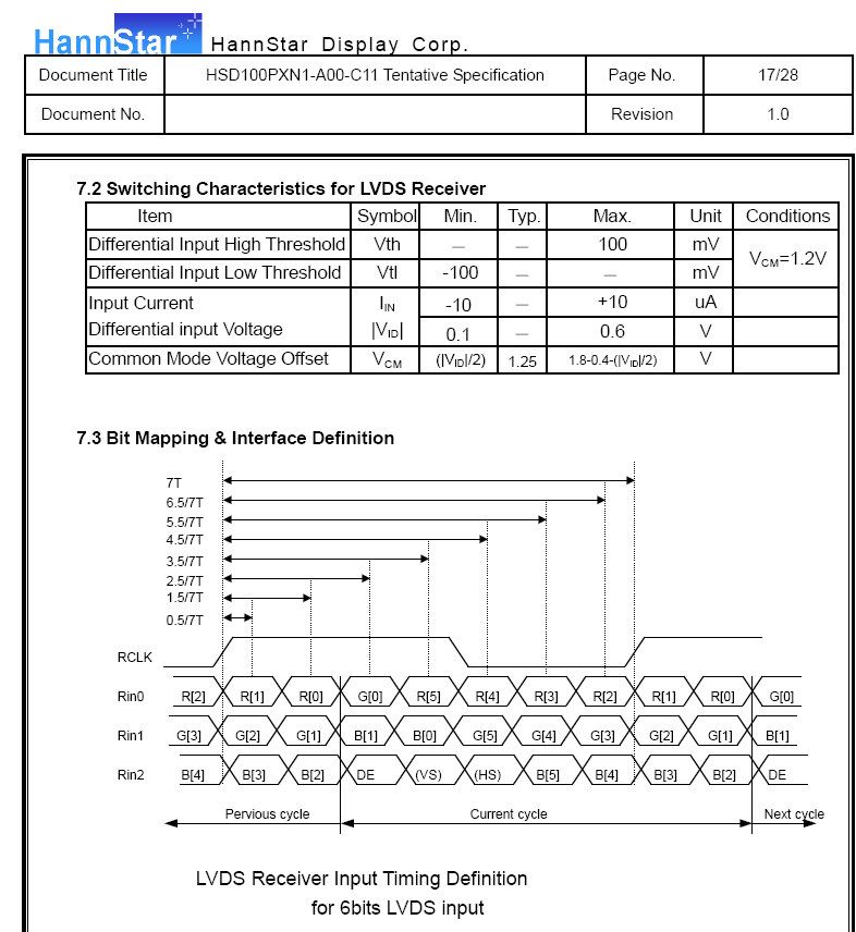
2. no, because according to LVDS mapping standards, DIx_SERIAL_CLK = LDB_DIx_SERIAL_CLK_ROOT
is clock for data serializing. For clock this is 1/7 (75.4MHz =528/7MHz),
please refer to example to datasheet HannStar LCD used on Sabre board p.17
https://community.freescale.com/message/331832#331832
Best regards
igor
-----------------------------------------------------------------------------------------------------------------------
Note: If this post answers your question, please click the Correct Answer button. Thank you!
-----------------------------------------------------------------------------------------------------------------------
Dear Igor,
Thank you for your reply.
I understood what I was wrong.
I misunderstood the clock for serializing is used for LVDS transfer also.
But actually, same lock frequency is used for transferring whether LCD interface is LVDS (serial) or parallel if resolution is same.
> 2. no, because according to LVDS mapping standards, DIx_SERIAL_CLK = LDB_DIx_SERIAL_CLK_ROOT
> is clock for data serializing.
OK, so which clock is user for LVDSx_CLK_P/LVDSx_CLK_N?
LDB_DIx_SERIAL_CLK_ROOT is used after divided in LDB?
Or db_dix_ipu is used?
Or other clock made by IPU counter is used?
Best Regards,
Satoshi Shimoda
