- Forums
- Product Forums
- General Purpose MicrocontrollersGeneral Purpose Microcontrollers
- i.MX Forumsi.MX Forums
- QorIQ Processing PlatformsQorIQ Processing Platforms
- Identification and SecurityIdentification and Security
- Power ManagementPower Management
- MCX Microcontrollers
- S32G
- S32K
- S32V
- MPC5xxx
- Other NXP Products
- Wireless Connectivity
- S12 / MagniV Microcontrollers
- Powertrain and Electrification Analog Drivers
- Sensors
- Vybrid Processors
- Digital Signal Controllers
- 8-bit Microcontrollers
- ColdFire/68K Microcontrollers and Processors
- PowerQUICC Processors
- OSBDM and TBDML
- S32M
-
- Solution Forums
- Software Forums
- MCUXpresso Software and ToolsMCUXpresso Software and Tools
- CodeWarriorCodeWarrior
- MQX Software SolutionsMQX Software Solutions
- Model-Based Design Toolbox (MBDT)Model-Based Design Toolbox (MBDT)
- FreeMASTER
- eIQ Machine Learning Software
- Embedded Software and Tools Clinic
- S32 SDK
- S32 Design Studio
- GUI Guider
- Zephyr Project
- Voice Technology
- Application Software Packs
- Secure Provisioning SDK (SPSDK)
- Processor Expert Software
- MCUXpresso Training Hub
-
- Topics
- Mobile Robotics - Drones and RoversMobile Robotics - Drones and Rovers
- NXP Training ContentNXP Training Content
- University ProgramsUniversity Programs
- Rapid IoT
- NXP Designs
- SafeAssure-Community
- OSS Security & Maintenance
- Using Our Community
-
- Cloud Lab Forums
-
- Knowledge Bases
- ARM Microcontrollers
- i.MX Processors
- Identification and Security
- Model-Based Design Toolbox (MBDT)
- QorIQ Processing Platforms
- S32 Automotive Processing Platform
- Wireless Connectivity
- CodeWarrior
- MCUXpresso Suite of Software and Tools
- MQX Software Solutions
-
- Home
- :
- QorIQプロセッシングプラットフォーム
- :
- Tシリーズ
- :
- Re: T1042 HRESET_B Negation Problem in Power On Reset Sequence
T1042 HRESET_B Negation Problem in Power On Reset Sequence
- RSS フィードを購読する
- トピックを新着としてマーク
- トピックを既読としてマーク
- このトピックを現在のユーザーにフロートします
- ブックマーク
- 購読
- ミュート
- 印刷用ページ
T1042 HRESET_B Negation Problem in Power On Reset Sequence
- 新着としてマーク
- ブックマーク
- 購読
- ミュート
- RSS フィードを購読する
- ハイライト
- 印刷
- 不適切なコンテンツを報告
Hi,
I am trying to bring up a custom T1042 CPU. During power-on reset sequence via driving hard-coded cfg_rcw_src pins (driven by the FPGA), a proper HRESET timing has been observed as shown in RM Figure 4-1. So I have burnt my custom RCW (to address 0xE800_0000) and uboot (to 0xEFF4_0000) to the NOR Flash by using CodeWarrior TAP(write operation is verified by CodeWarrior and data is manually checked by checking hexdump from Flash locations).
However, when the cfg_rcw_src option that addresses NOR Flash is driven on IFC interface, CPU asserts HRESET_B but does not negates. Also RST_REQ_B and CPU_ASLEEP does not follow the reference timing. When CPU's internal registers are checked via CodeWarrior TAP in debug mode the expected cfg_rcw_src (0x27 for NOR Flash) and other conf inputs (eng_use_0/1/2, ifc_te, dram_type) are seen as they got sampled correct. Also, while in debug mode, by clicking resume and suspend right after it makes us see output at the serial for uboot. What could be the reason that avoids the sequence to be done?
Edit:
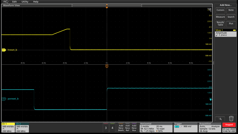
Please see the values of the used configuration inputs' POR values and attached scope capturings of the them with respect to PORESET_B deassertion:
- cfg_rcw_src[0:8] = 0_0010_0111 - (rcw_srcn_10cyc_wrt_poreset.png)
- eng_use_0/1/2 = 1 - 100 MHz single ended clk is given (eng_use_1us_wrt_poreset.png)
- ifc_te = 0,
- dram_type = 0
Previously, I said there was no activity on IFC_A & IFC_AD buses after PORESET_B is deasserted and IFC pins are released to high-Z by FPGA. However, I realized there are some (and last) attempts on cfg_rcw_src pins. In similar amounts of time after low-to-high transition of PORESET_B, there happens some assertions. Please see attached srcn_activity.png and IFC_OE_B_activity.png files.
Regards,
Oguzhan
- 新着としてマーク
- ブックマーク
- 購読
- ミュート
- RSS フィードを購読する
- ハイライト
- 印刷
- 不適切なコンテンツを報告
Hello ufedor,
This problem is solved. The reason is, board signals are not working properly during power on sequence IF Code Warrior tab is connected to our custom board. We were also writing to 0xE800_0000 until last week.
Writing RCW to 0xE000_0000 and removing CW TAB before POR did fix the problem.
- 新着としてマーク
- ブックマーク
- 購読
- ミュート
- RSS フィードを購読する
- ハイライト
- 印刷
- 不適切なコンテンツを報告
U-Boot relocation is performed by relative addressing (not absolute).
- 新着としてマーク
- ブックマーク
- 購読
- ミュート
- RSS フィードを購読する
- ハイライト
- 印刷
- 不適切なコンテンツを報告
Hello ufedor,
I do not see the name of my custom boards nor flash device on this list. I was using default configuration of Code Warrior while doing flash programming. I will write my RCW on 0xE000_0000 but I just realized this. Can this situation cause a problem ? Or just aligning base from 0xE8000_0000 to 0xE000_0000 on 'Base Address' column is simple enough ?
Thanks, Regards.
- 新着としてマーク
- ブックマーク
- 購読
- ミュート
- RSS フィードを購読する
- ハイライト
- 印刷
- 不適切なコンテンツを報告
The NOR Flash IFC chip-select has to be modified for base address 0xE0000000.
RCW also has to be programmed to 0xE0000000.
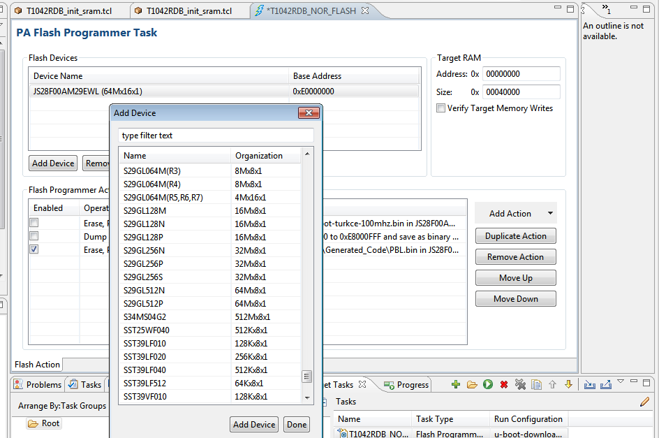
In the Flash Programmer it is possible to select 128MB NOR Flash.
- 新着としてマーク
- ブックマーク
- 購読
- ミュート
- RSS フィードを購読する
- ハイライト
- 印刷
- 不適切なコンテンツを報告
Hello ufedor,
The default flash device is "JS28F00AM29EWL" when I import T1042D4RDB NOR Flash Programming options.
In our design we used "S70GL02GS" (https://www.cypress.com/documentation/datasheets/s70gl02gs-2gbit-256mbytes-30v-flash-memory ) refer here.
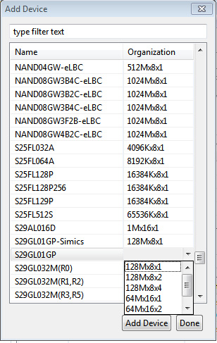
Which flash device option is recommended for "S70GL02GS". I couln't find it on the Devices list opened with "Add Device" Button.
S29GL01GP seems the closest configuration for our device but It does not have "128Mx16x2" option.
- 新着としてマーク
- ブックマーク
- 購読
- ミュート
- RSS フィードを購読する
- ハイライト
- 印刷
- 不適切なコンテンツを報告
> "128Mx16x2"
This means 32-bit-wide data bus, but IFC has only 16 AD lines.
You wrote:
> I have burnt my custom RCW (to address 0xE800_0000) and uboot (to 0xEFF4_0000)
> to the NOR Flash by using CodeWarrior
Which NOR Flash was selected?
- 新着としてマーク
- ブックマーク
- 購読
- ミュート
- RSS フィードを購読する
- ハイライト
- 印刷
- 不適切なコンテンツを報告
Hello,
>This means 32-bit-wide data bus, but IFC has only 16 AD lines.
I thought that means 128 Megaybte, 16 bit width with 2 nor flash (total: 256 Megabyte) chip configuration. So in this case, 16x1 means 16 bit width data bus, then what is the meaning of 64M or 128M ?
>You wrote:
>> I have burnt my custom RCW (to address 0xE800_0000) and uboot (to 0xEFF4_0000)
>> to the NOR Flash by using CodeWarrior
>Which NOR Flash was selected?
It was default (JS28F00AM29EWL 64x16x1) and it was working with succeded feedback logs on code warrior console. I also checked with Flash Dump actions, RCW and U-boot was writing without any error and written data was correct (0xE000_0000 and 0xE800_0000 has RCW data, 0xEFF4_0000 has U-boot data). I am also able to write 0xE000_0000 by selecting "JS28F00AM29EWL 64x16x1" and writing "0xE000_0000" to Base Address column.
I just wanted to be sure that using different device name configuration ("JS28F00AM29EWL") with my own device ("S70GL02GS") can be the reason of this rcw reading problem ?
EDIT: The device configuration named "SL29GL01GP 64x16x1" is also working (tried with dump flash, program/verify and erase commands).
I also get confused about that, Flash Dump action is working well with all the addresses that I want to check. Code Warrior TAB is writing/reading from NOR flash correctly. Can we still say that we can not read RCW from NOR Flash during POWER ON RESET SEQUENCE ?
Thanks.
- 新着としてマーク
- ブックマーク
- 購読
- ミュート
- RSS フィードを購読する
- ハイライト
- 印刷
- 不適切なコンテンツを報告
> It was default (JS28F00AM29EWL 64x16x1)
Use this selection and program RCW to 0xE0000000.
- 新着としてマーク
- ブックマーク
- 購読
- ミュート
- RSS フィードを購読する
- ハイライト
- 印刷
- 不適切なコンテンツを報告
Yes, this is a problem.
For the 256MB Flash the RCW programming address has to be 0xE0000000 because in the Power Architecture each window must be aligned to its size.
In the specific case the RCW was written to the middle of the NOR Flash device, but during boot physical offset 0 is used to read RCW.
- 新着としてマーク
- ブックマーク
- 購読
- ミュート
- RSS フィードを購読する
- ハイライト
- 印刷
- 不適切なコンテンツを報告
Thanks for the reply,
In this case, I assume a new .tcl file is needed to apply law entry between 0xE000_0000 and 0xEFFF_FFFF,
Does U-boot also need a relocation (writing to 0xE7F4_000 instead of 0xEFF4_0000)?
Regards.
- 新着としてマーク
- ブックマーク
- 購読
- ミュート
- RSS フィードを購読する
- ハイライト
- 印刷
- 不適切なコンテンツを報告
The requested traces must simultaneously show:
a) low->high edge of PORESET_B
b) {IFC_AD[8:15], IFC_CLE}
c) 6-8 SYSCLK cycles after the low->high edge of PORESET_B
- 新着としてマーク
- ブックマーク
- 購読
- ミュート
- RSS フィードを購読する
- ハイライト
- 印刷
- 不適切なコンテンツを報告
Sorry but due to incapableness of touching those pads in the same time, I did separate the scope shots each other yet sampling every one of them with respect to PORESET_B's low->high edge.
- sysclk.png shows used 100MHz clock input to have a reference for IFC_AD[8:15] (IFC_CLE is unfortunately untouchable due design)
- IFC_AD[8:15] = rcw_srcn_10cyc_wrt_poreset.png shots have 20ns/div sample rate so roughly represents 2 sysclk cycles. So I've taken scope shots for 10 cycles long before and after PORESET_B low to high based trigger setting.
If it is still not sufficient, please paraphrase the requirements to avoid our misunderstanding.
- 新着としてマーク
- ブックマーク
- 購読
- ミュート
- RSS フィードを購読する
- ハイライト
- 印刷
- 不適切なコンテンツを報告
Where is rcw_src8?
The RESET_REQ_B is asserted after ~500us after PORESET_B is deasserted which could correspond to a PLL inability to lock.
Which exactly RCW binary image is used?
Which clocks (frequencies) are applied to the processor?
- 新着としてマーク
- ブックマーク
- 購読
- ミュート
- RSS フィードを購読する
- ハイライト
- 印刷
- 不適切なコンテンツを報告
- 新着としてマーク
- ブックマーク
- 購読
- ミュート
- RSS フィードを購読する
- ハイライト
- 印刷
- 不適切なコンテンツを報告
What is the SerDes reference clock(s) frequency?
- 新着としてマーク
- ブックマーク
- 購読
- ミュート
- RSS フィードを購読する
- ハイライト
- 印刷
- 不適切なコンテンツを報告
Until now SerDes reference clocks were not given (SD1_REF_CLKx_P/N pins were left floating since the oscillator is not programmed).
Also the clock signals;
- DIFF_SYSCLK/_B,
- SD1_REF_CLKx_P/N,
were not pulled down but floating.
So now, as denoted in Design Checklist - AN4825 these pins are connected to GND. And also I made some changes in RCW like both PLLs are programmed to be powered down. (not sure if at least one of the PLLs has to be used for PoR sequence)
- 新着としてマーク
- ブックマーク
- 購読
- ミュート
- RSS フィードを購読する
- ハイライト
- 印刷
- 不適切なコンテンツを報告
> both PLLs are programmed to be powered down
Do you see RESET_REQ_B still asserted with this RCW?
- 新着としてマーク
- ブックマーク
- 購読
- ミュート
- RSS フィードを購読する
- ハイライト
- 印刷
- 不適切なコンテンツを報告
Yes, unfortunately.
- 新着としてマーク
- ブックマーク
- 購読
- ミュート
- RSS フィードを購読する
- ハイライト
- 印刷
- 不適切なコンテンツを報告
Please use the scope to ensure that RCW is correctly read from the NOR Flash.
Also ensure that all signals having note 5 in the QorIQ T1042, T1022 Data Sheet, Table 1. Pinout list by bus are not pulled low during POR.
- 新着としてマーク
- ブックマーク
- 購読
- ミュート
- RSS フィードを購読する
- ハイライト
- 印刷
- 不適切なコンテンツを報告
The note 5 of from Table 1 in datasheet is already satisfied. And please see the attached scope shots (srcn_activity.png files) of the question which shows the attempt of (cfg_rcw_src[0:4]) IFC interface to read RCW. After ~445 us (under 100 MHz SYSCLK) from PORESET_B's negation there seen two consecutive activity on these buses.
Can we still have a suspicion on PLL lock issue at this point? Would IFC interface start to assert its pins without verifying PLLs are locked?
Does CPU require at least one of the SerDes REF clocks (SD1_REF_CLKn_P/N) to be given properly?


