- Forums
- Product Forums
- General Purpose MicrocontrollersGeneral Purpose Microcontrollers
- i.MX Forumsi.MX Forums
- QorIQ Processing PlatformsQorIQ Processing Platforms
- Identification and SecurityIdentification and Security
- Power ManagementPower Management
- Wireless ConnectivityWireless Connectivity
- RFID / NFCRFID / NFC
- MCX Microcontrollers
- S32G
- S32K
- S32V
- MPC5xxx
- Other NXP Products
- S12 / MagniV Microcontrollers
- Powertrain and Electrification Analog Drivers
- Sensors
- Vybrid Processors
- Digital Signal Controllers
- 8-bit Microcontrollers
- ColdFire/68K Microcontrollers and Processors
- PowerQUICC Processors
- OSBDM and TBDML
- S32M
-
- Solution Forums
- Software Forums
- MCUXpresso Software and ToolsMCUXpresso Software and Tools
- CodeWarriorCodeWarrior
- MQX Software SolutionsMQX Software Solutions
- Model-Based Design Toolbox (MBDT)Model-Based Design Toolbox (MBDT)
- FreeMASTER
- eIQ Machine Learning Software
- Embedded Software and Tools Clinic
- S32 SDK
- S32 Design Studio
- GUI Guider
- Zephyr Project
- Voice Technology
- Application Software Packs
- Secure Provisioning SDK (SPSDK)
- Processor Expert Software
-
- Topics
- Mobile Robotics - Drones and RoversMobile Robotics - Drones and Rovers
- NXP Training ContentNXP Training Content
- University ProgramsUniversity Programs
- Rapid IoT
- NXP Designs
- SafeAssure-Community
- OSS Security & Maintenance
- Using Our Community
-
- Cloud Lab Forums
-
- Knowledge Bases
- ARM Microcontrollers
- i.MX Processors
- Identification and Security
- Model-Based Design Toolbox (MBDT)
- QorIQ Processing Platforms
- S32 Automotive Processing Platform
- Wireless Connectivity
- CodeWarrior
- MCUXpresso Suite of Software and Tools
- MQX Software Solutions
-
- Home
- :
- Product Forums
- :
- Sensors
- :
- Re: Why MMA9555 's Pin1 ID is shortened to Pin1?
Why MMA9555 's Pin1 ID is shortened to Pin1?
- Subscribe to RSS Feed
- Mark Topic as New
- Mark Topic as Read
- Float this Topic for Current User
- Bookmark
- Subscribe
- Mute
- Printer Friendly Page
- Mark as New
- Bookmark
- Subscribe
- Mute
- Subscribe to RSS Feed
- Permalink
- Report Inappropriate Content
Hi everybody,
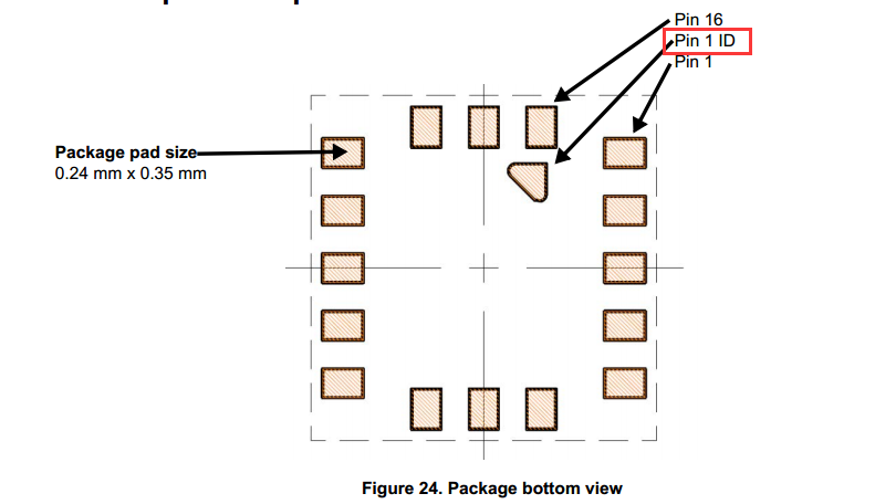
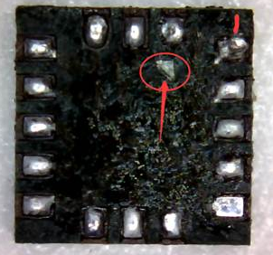
I found MMA9555's Pin1 ID is shortened to Pin1. Actually the resistor between them is 0.3Ω. Do you know what's the reason?
I don't find any description about Pin1 ID in datasheet. Generally speeking, this pin should be just an identification. I don't understand why it connect to VDD.
Any comments would be appreciated.
Solved! Go to Solution.
- Mark as New
- Bookmark
- Subscribe
- Mute
- Subscribe to RSS Feed
- Permalink
- Report Inappropriate Content
Hi Wenxue,
This is due to the layout of device package substrate: pin 1 ID is connected to pin 1 through the bottom layer of this LGA substrate.
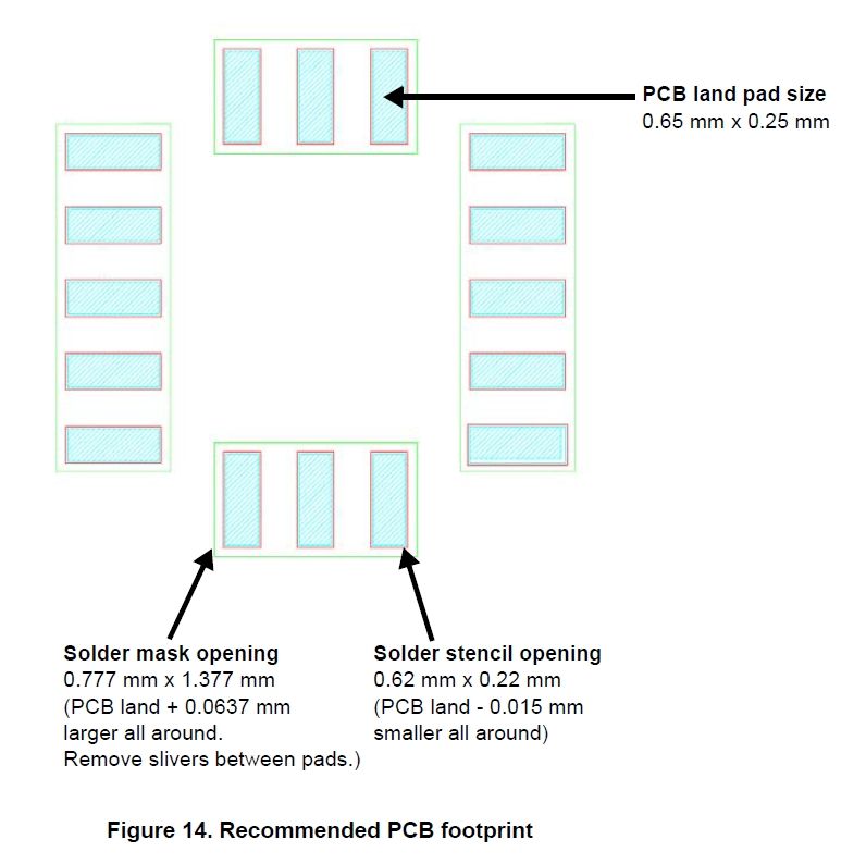
Datasheet provides footprint and land pattern information which keep pin 1 ID unconnected. Did you experienced any issue when mounting the part ?
Regards, Jacques.
- Mark as New
- Bookmark
- Subscribe
- Mute
- Subscribe to RSS Feed
- Permalink
- Report Inappropriate Content
Hi Jacques,
Yes, a customer meet an issue when mounting the part. Customer designed a pad in the bottom of the chip, and the pad is connected to GND. So Pin1 VDD is shortened to GND in this case.
Datasheet don’t have any information indicate Pin1 ID is shortened to GND. I think we need describe it clearly.
Best Regards,
Wenxue
- Mark as New
- Bookmark
- Subscribe
- Mute
- Subscribe to RSS Feed
- Permalink
- Report Inappropriate Content
Hi Wenxue,
I'm surprised the customer introduced a GND pad under the package.
Figure 14 and 13 in Datasheet are providing clear description of solder mask and stencil opening.
Anyway, we'll add a word of caution about pin 1 ID in a subsequent revision of the datasheet.
Thanks for raising this concern, Jacques.


