- Forums
- Product Forums
- General Purpose MicrocontrollersGeneral Purpose Microcontrollers
- i.MX Forumsi.MX Forums
- QorIQ Processing PlatformsQorIQ Processing Platforms
- Identification and SecurityIdentification and Security
- Power ManagementPower Management
- MCX Microcontrollers
- S32G
- S32K
- S32V
- MPC5xxx
- Other NXP Products
- Wireless Connectivity
- S12 / MagniV Microcontrollers
- Powertrain and Electrification Analog Drivers
- Sensors
- Vybrid Processors
- Digital Signal Controllers
- 8-bit Microcontrollers
- ColdFire/68K Microcontrollers and Processors
- PowerQUICC Processors
- OSBDM and TBDML
- S32M
-
- Solution Forums
- Software Forums
- MCUXpresso Software and ToolsMCUXpresso Software and Tools
- CodeWarriorCodeWarrior
- MQX Software SolutionsMQX Software Solutions
- Model-Based Design Toolbox (MBDT)Model-Based Design Toolbox (MBDT)
- FreeMASTER
- eIQ Machine Learning Software
- Embedded Software and Tools Clinic
- S32 SDK
- S32 Design Studio
- GUI Guider
- Zephyr Project
- Voice Technology
- Application Software Packs
- Secure Provisioning SDK (SPSDK)
- Processor Expert Software
- MCUXpresso Training Hub
-
- Topics
- Mobile Robotics - Drones and RoversMobile Robotics - Drones and Rovers
- NXP Training ContentNXP Training Content
- University ProgramsUniversity Programs
- Rapid IoT
- NXP Designs
- SafeAssure-Community
- OSS Security & Maintenance
- Using Our Community
-
- Cloud Lab Forums
-
- Knowledge Bases
- ARM Microcontrollers
- i.MX Processors
- Identification and Security
- Model-Based Design Toolbox (MBDT)
- QorIQ Processing Platforms
- S32 Automotive Processing Platform
- Wireless Connectivity
- CodeWarrior
- MCUXpresso Suite of Software and Tools
- MQX Software Solutions
-
- Home
- :
- Product Forums
- :
- S12 / MagniV Microcontrollers
- :
- Waveform of HSX and HGX at the moment after power on
Waveform of HSX and HGX at the moment after power on
- Subscribe to RSS Feed
- Mark Topic as New
- Mark Topic as Read
- Float this Topic for Current User
- Bookmark
- Subscribe
- Mute
- Printer Friendly Page
Waveform of HSX and HGX at the moment after power on
- Mark as New
- Bookmark
- Subscribe
- Mute
- Subscribe to RSS Feed
- Permalink
- Report Inappropriate Content
There is a new MCU without software. I have done several tests to capture the waveform of the HSX and HGX at the moment after power on.
Connect the circuit as shown, VBAT=12V,CBS=470nf,RFILT=47Ω,RHS=10Ω,CFILT=NC:
- At the moment after power on, HSX rises up to 11V at the same speed with VLS_OUT, and then falls to 0V after about 45ms. The waveform of HGX is completely consistent with HSX;
- In the case of removing RHS, HSX remains low and HGX is also low after power on.
Questions:
- As the normal circuit, whether HSX and HGX are connected at the moment after power on?
- In the case of removing RHS, I guess the connect between HSX and HGX is disappeared and the MCU changes HGX to 0V. The reason is that HGX will be 11V due to CG when in pending state. But I cannot find specification about the principle of changing HGX to 0V in the datasheet.
Look forward to your reply and thanks very much!
- Mark as New
- Bookmark
- Subscribe
- Mute
- Subscribe to RSS Feed
- Permalink
- Report Inappropriate Content
Hi,
The behavior is expected.
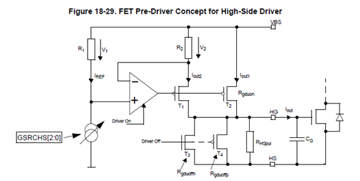
When the drivers are off, V_HSx = V_HGx, they are connected internally (RHSpul, S12ZVM RM, Table E-1, #6).
The FETs act like capacitive dividers. On power-on, the phase signal (HSx) goes up and this is what it is observed on HGx. It is then slowly discharge to ground.
BR, Daniel
- Mark as New
- Bookmark
- Subscribe
- Mute
- Subscribe to RSS Feed
- Permalink
- Report Inappropriate Content
- Mark as New
- Bookmark
- Subscribe
- Mute
- Subscribe to RSS Feed
- Permalink
- Report Inappropriate Content
Hi,
You are right, this is not just the RHSpul, this resistor is there to ensure the pins are shorted when the GDU is disabled.
When enabled and the HS drivers are OFF, the pins get shorted as shown below.
The pins are shorted together but the HGx pin is not driven to the ground, the pulse voltage drops due to leakage currents on the pins.
Regarding CBS, I’m not sure, let me check.
Where did you get the HSx/HGx impendance to GND?
Thanks,
BR, Daniel
- Mark as New
- Bookmark
- Subscribe
- Mute
- Subscribe to RSS Feed
- Permalink
- Report Inappropriate Content
Hi,
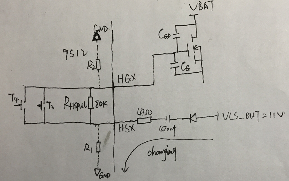
You means the transistors T3 and T4 is switch on at the moment after power on, because GDU or HS driver is disabled. So HGx and HSx are shorted.
While normal circuit, HGx is shorted to HSx, but HGx is not driven to ground, so the voltage on the pin drops due to leakage current. Your description is right.
In the case of removing RHS, I guess HGX is driven to ground, because if HGx were floating, it will be 11V due to CGS and CGD. But I cannot find specification or diagram about the principle of driven HGX toground in the datasheet. This question is crucial.
Regarding the HSx and HGx impedance to GND, I got it on the pins by multimeter when power off, removing external components.
Thanks !
Best Regards!
王 震/Wang Zhen
发件人: danielmartynek
发送时间: 2019年4月10日 22:39
收件人: Wang Zhen王震
主题: Re: - Re: Waveform of HSX and HGX at the moment after power on
NXP Community <https://community.freescale.com/resources/statics/1000/35400-NXP-Community-Email-banner-600x75.jpg>
Re: Waveform of HSX and HGX at the moment after power on
reply from Daniel Martynek<https://community.nxp.com/people/danielmartynek?et=watches.email.thread> in S12 / MagniV Microcontrollers - View the full discussion<https://community.nxp.com/message/1137524?commentID=1137524&et=watches.email.thread#comment-1137524>
- Mark as New
- Bookmark
- Subscribe
- Mute
- Subscribe to RSS Feed
- Permalink
- Report Inappropriate Content
Hi and sorry for the delay.
If the RHS is removed from you circuit below, the HS driver is not powered from VLS_OUT and the energy from the HGx pin is stored in the HS driver and the voltage gets clamped on the HGx pin.
Hope it helps,
Daniel
- Mark as New
- Bookmark
- Subscribe
- Mute
- Subscribe to RSS Feed
- Permalink
- Report Inappropriate Content
Thanks for your reply!
Your analysis about the model of MOSFET is obsolutely right. But I have several questions about the circuit of the charging and discharging.
Firstly I think that falling-down of HSx results from charging of CBS.
Then if HSx is connected to HGx by RHSpul, HGx will not be 11V due to divider between RHSpul and R2. As the question a) I think that HSx is connected to HGx by lower impedance or directly.
Finally I also look foreword to the answer of question b) !
Thank you very much!
获取 Outlook for iOS<https://aka.ms/o0ukef>


