- Forums
- Product Forums
- General Purpose MicrocontrollersGeneral Purpose Microcontrollers
- i.MX Forumsi.MX Forums
- QorIQ Processing PlatformsQorIQ Processing Platforms
- Identification and SecurityIdentification and Security
- Power ManagementPower Management
- MCX Microcontrollers
- S32G
- S32K
- S32V
- MPC5xxx
- Other NXP Products
- Wireless Connectivity
- S12 / MagniV Microcontrollers
- Powertrain and Electrification Analog Drivers
- Sensors
- Vybrid Processors
- Digital Signal Controllers
- 8-bit Microcontrollers
- ColdFire/68K Microcontrollers and Processors
- PowerQUICC Processors
- OSBDM and TBDML
- S32M
-
- Solution Forums
- Software Forums
- MCUXpresso Software and ToolsMCUXpresso Software and Tools
- CodeWarriorCodeWarrior
- MQX Software SolutionsMQX Software Solutions
- Model-Based Design Toolbox (MBDT)Model-Based Design Toolbox (MBDT)
- FreeMASTER
- eIQ Machine Learning Software
- Embedded Software and Tools Clinic
- S32 SDK
- S32 Design Studio
- GUI Guider
- Zephyr Project
- Voice Technology
- Application Software Packs
- Secure Provisioning SDK (SPSDK)
- Processor Expert Software
- MCUXpresso Training Hub
-
- Topics
- Mobile Robotics - Drones and RoversMobile Robotics - Drones and Rovers
- NXP Training ContentNXP Training Content
- University ProgramsUniversity Programs
- Rapid IoT
- NXP Designs
- SafeAssure-Community
- OSS Security & Maintenance
- Using Our Community
-
- Cloud Lab Forums
-
- Knowledge Bases
- ARM Microcontrollers
- i.MX Processors
- Identification and Security
- Model-Based Design Toolbox (MBDT)
- QorIQ Processing Platforms
- S32 Automotive Processing Platform
- Wireless Connectivity
- CodeWarrior
- MCUXpresso Suite of Software and Tools
- MQX Software Solutions
-
- Home
- :
- Product Forums
- :
- S12 / MagniV Microcontrollers
- :
- Re: Help trying to understand memory Paging
Help trying to understand memory Paging
- Subscribe to RSS Feed
- Mark Topic as New
- Mark Topic as Read
- Float this Topic for Current User
- Bookmark
- Subscribe
- Mute
- Printer Friendly Page
Help trying to understand memory Paging
- Mark as New
- Bookmark
- Subscribe
- Mute
- Subscribe to RSS Feed
- Permalink
- Report Inappropriate Content
I am tring to understand how the CPU12 handles paging. We are using the MC9S12XEQ512.
When you have an instruction like LDY $1000, $1000 is located in paged RAM section of the memory map so I assumed that if RPAGE was set to F9 and you called LDY $1000, it would load the value at ram location 0xF9000.
If you want to access ram in page FA, I assumed the compiler would generate code to set RPAGE to FA and then also access the same memory area $1000.
However looking at my compiler output it still sets RPAGE to F9 and then accesses address $2000
LDY $2000
But according to the data sheet, $2000 is non-paged RAM (or ram at page 0xFE)
So I do not understand how this works. Can someone shine so light on this for me?
Thanks
Shawn
- Mark as New
- Bookmark
- Subscribe
- Mute
- Subscribe to RSS Feed
- Permalink
- Report Inappropriate Content
Thanks for the Excel file.
Sorry, I am still not getting it.
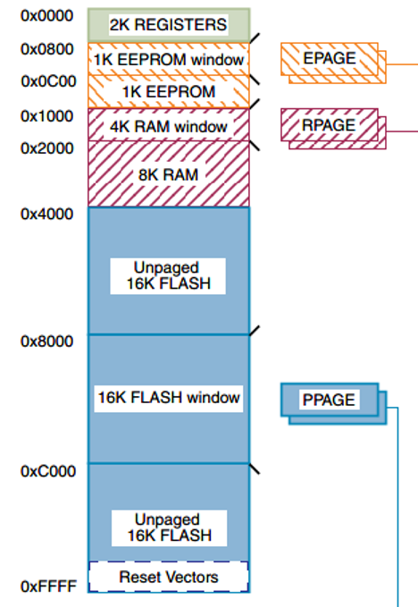
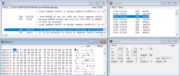
For the flash window I was just getting that from this image
I wrote a very simple program in assembly
LDAA #0F9H ;get rpage value F9
STAA _RPAGE ;write to rpage
LDD #1234H
STD $1000
LDD #1235H
STD $2000
LDD #1236H
STD $3000
LDD #1237H
STD $4000
LDD #1238H
STD $5000
LDD #1239H
STD $6000
LDD #123AH
STD $7000
LDD #123BH
STD $8000
Accroding to your exel file, when I write to $2000 it shoud write to $0F_E000 but it actualey writes to $0F_A000
Accroding to your exel file, when I write to $3000 it shoud write to $0F_F000 but it actualey writes to $0F_B000
I tried these combinations
Set RPAGE to F9
Write Local Address | Global Address of write |
1000 | F9000 |
2000 | FA000 |
3000 | FB000 |
4000 | FC000 |
5000 | FD000 |
6000 | FE000 |
7000 | FF000 |
8000 | ?????? |
Set RPAGE to FB
Write Local Address | Global Address of write |
1000 | FB000 |
2000 | FA000 |
3000 | FB000 |
4000 | FC000 |
5000 | FD000 |
6000 | FE000 |
7000 | FF000 |
8000 | ?????? |
Set RPAGE to F8
Write Local Address | Global Address of write |
1000 | F9000 |
2000 | FA000 |
3000 | FB000 |
4000 | FC000 |
5000 | FD000 |
6000 | FE000 |
7000 | FF000 |
8000 | ?????? |
Does these tables make sense? It seems like local address $2000 to $7FFF write to RAM at $0F_A000 to $0F_FFFF and I do not understand why.
- Mark as New
- Bookmark
- Subscribe
- Mute
- Subscribe to RSS Feed
- Permalink
- Report Inappropriate Content
Hi,
I do not know how you are reading and check the data. I suggest you to use either address 0xF91000'L or 0x0F9000'G to the debugger recognizes which memory space you want to access. The debugger does not considers memory window, you have to confirm it by 'G or 'L.
I have rewritten your code to the CodeWarrior asm project with comments and it is:
LDAA #$F9 ; write RPAGE = 0xF9
STAA RPAGE
LDD #$1234 ; write rpage_off = 0xF91000 == gpage_off = 0x0F9000
STD $1000
LDD #$1235 ; even RPAGE is set for 0xF9 the local address 0x2000 will be written
STD $2000 ; because RPAGE window can only be 1000-1FFF so RPAGE is not counted into access and
; it will be written:
; local addres 0x2000 or global addres 0x0FE000'G or rpage_off 0xFE1000
LDD #$1236 ; even RPAGE is set for 0xF9 the local address 0x3000 will be written
STD $3000 ; because RPAGE window can only be 1000-1FFF so RPAGE is not counted into access and
; it will be written:
; local addres 0x3000 or global addres 0x0FF000'G or rpage_off 0xFF1000
LDD #$1236 ; it is nonsense because even everything as in previous case is valid but
STD $4000 ; it is not possible to write to address 0x4000 because it is nonpaged flash address space
LDD #$1236 ; it is nonsense because even everything as in previous case is valid but
STD $5000 ; it is not possible to write to address 0x5000 because it is nonpaged flash address space
LDD #$1236 ; it is nonsense because even everything as in previous case is valid but
STD $6000 ; it is not possible to write to address 0x6000 because it is nonpaged flash address space
LDD #$1236 ; it is nonsense because even everything as in previous case is valid but
STD $7000 ; it is not possible to write to address 0x7000 because it is nonpaged flash address space
LDD #$1236 ; it is nonsense because you are trying to write to a flash space given by address PPAGE_off
STD $8000 ; because you set offset from PPAGE paged window 8000-BFFF
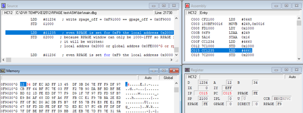
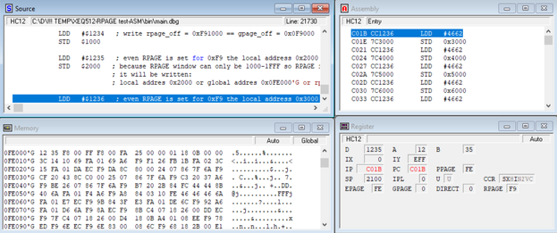
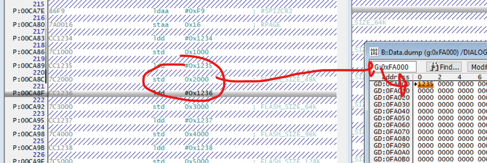
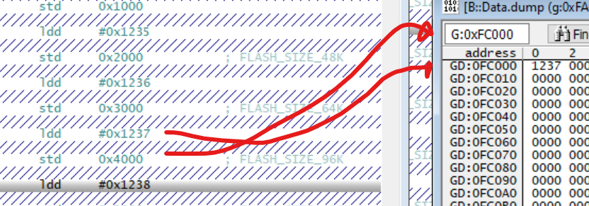
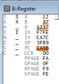
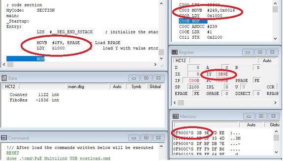
The result for the first three working and correct approaches are here>
1)
2)
3)
It is necessary to think only on the last 16 bits and this value select the addressing mode whether it will be near 6 bit address only or it will be RPAGE used or PPAGE or EPAGE. I do not want to talk about GPAGE now. (GPAGE is used with as instructins GLD GLS)
*******************************************
I do not want but I suppose I will confuse you. There is one memory space with overlaps when you use short addressing mode with addresses 0x4000-0x7FFF. This address space can either address internal RAM or external bus or internal Flash. It is always necessary to think about global address space to understand the placement because it is linear and nothing overlaps. The address space 0x4000-0x7FFF is good to be think about if you want to access this RAM space – of course, if it is defined in the device, or if you have confusing existence and access in the case of phantom device.
I forget to mention. Some XEQ512 devices were made as a phantoms of XEP100 devices which has master set of peripherals and memory map. The phantom is created by simple definition of smaller memory map and less amount of peripherals or reduced features even it is the same device like “master” device. However, the phantom is not allowed to be used like a master device – loss of guarantee – the reason is that undefined peripherals o memory have limited tests so they do not have full guarantee.
I have attached the memory map of the master device. You can see it has also addresses 4000-5000 and 6000-7000 in the memory map of the RAM.
What is important is that the part 4000-7000 can be visible in the memory map as unpaged RAM or as a unpaged flash.
The reference manual….
RAMHM
RAM only in higher Half of the memory map
Write: Once in normal and emulation modes and anytime in special modes
0 Accesses to $4000–$7FFF will be mapped to $14_4000-$14_7FFF in the global memory space (external
access).
1 Accesses to $4000–$7FFF will be mapped to $0F_C000-$0F_FFFF in the global memory space (RAM area).
ROMHM
FLASH or ROM only in higher Half of Memory Map
Write: Once in normal and emulation modes and anytime in special modes
0 The fixed page of Flash or ROM can be accessed in the lower half of the memory map. Accesses to
0x4000–0x7FFF will be mapped to 0x7F_4000-0x7F_7FFF in the global memory space.
1 Disables access to the Flash or ROM in the lower half of the memory map.These physical locations of the
Flash or ROM can still be accessed through the program page window. Accesses to 0x4000–0x7FFF will be
mapped to 0x14_4000-0x14_7FFF in the global memory space (external access).
So, reset status of RAMHM = 0. It means, accesses to 0x4000–0x7FFF will be mapped to 0x144000-0x147FFF in the global memory space and address appears on the external bus – you access a memory at external bus .
If you change RAMHM = 1. It means, accesses to 0x4000–0x7FFF will be mapped to 0x0FC000-0x0FFFFF in the global memory space and address appears in the RAM space – you access the internal RAM memory.
Reset status of ROMHM = 0. It defines where the short flash 0x4000-0x7FFF will be mapped. When this bit is 0 then the MCU will read at the address 4000-7FFF is visible as a flash and can be accessed with short addresses 4000-7FFF and Global addresses 0x7F4000-0x7F7FFF and PPAGE address 0xFD8000-0xFDBFFF.
However, if you set ROMHM=1, the direct short access to the flash 0x4000 – 0x7FFF disappears and you still access this flash by Global addresses 0x7F4000-0x7F7FFF and PPAGE address 0xFD8000-0xFDBFFF. This s used when you want to use address 0x4000-0x7FFF as a address space for RAM.
Best regards,
Ladislav
- Mark as New
- Bookmark
- Subscribe
- Mute
- Subscribe to RSS Feed
- Permalink
- Report Inappropriate Content
What you describe in the test you ran is exactly what I expected to happen but that is not what is happening for me. And thus the confusion I am having
Unfortunatley, I am not using the NXP compiler. We use Cosmic compiler and Lauterbach debugger.
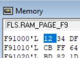
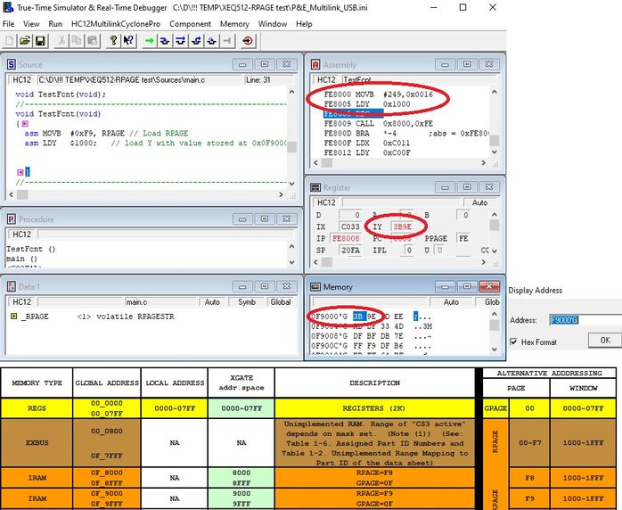
In the picture below you can see I have just writted to address $2000, which should go to FE000, the memory modified is at global address $FA000
And writing to $4000, which should not work, goes to FC000
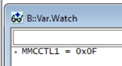
RAMHM and ROMHM both set. So maybe this explains why I can write to $4000, but does not explain why writing to $2000 goes to $FA000 and not $FE000.
- Tags:
- I am not using the NXP compiler. We use Cosmic compiler and Lauterbach debugger. In the picture below you can see I have just writted to address $2000 and the memory modified is at global address $FA000
- What you describe in the test you ran is exactly what I expected to happen but that is not what is happening for me. And thus the confusion I am having Unfortunatley
- Mark as New
- Bookmark
- Subscribe
- Mute
- Subscribe to RSS Feed
- Permalink
- Report Inappropriate Content
Hi,
I am sorry, in this case I think would be better to contact Lauterbach support.
The assembly code looks correct so the issue could be incorrect memory interpretation in Lauterbach.
However, what is the value in the MMCCTL1?
Best regards,
Ladislav
- Mark as New
- Bookmark
- Subscribe
- Mute
- Subscribe to RSS Feed
- Permalink
- Report Inappropriate Content
Hi,
Could you please look at the attached memory map. There is no duplicated address memory space. If the address does not exist internally then it is directed to the external bus.
Each line in the memory map presents addressing possibilities.
You can also force the compiler to use specific addressing mode by definition of address space and variable. For example if you create global space in the prm file and you put a far variable into this space it will be accessed by global address. The same you can do for RPAGE or Local space if required.
The flash 4000-7FFF is not a window.
If you look at the line 162,163 then the same address will be accessed if you access, for example,
0x4000 (near address) or
0x7F_4000 (far address uses global access instructions GLD..) or
0xFD8000 (far address but the mcu sees the address uses offset from 8000~BFFF so address is created with PPAGE_offset) Note, the PPAGE is usually used only for program access so flash data are read by global addressing or some spaces can be addressed by near address (4000-7FFF, C000-FFFF) The reason is that the PPAGE is used for program addressing so if you want to read data from flash you have to use code running out of different memory or unpaged space of the flash. Can be seen in the example XEP100-FLASH-PFLASH_reading-CW47
The same is valid for RAM and EEPROM but window for PAGE_ofseet addres in in different range.
GPAGE addressing mode is useable if we want to access linear space of larger than window (for given memory) size.
Best regards,
Ladislav
- Mark as New
- Bookmark
- Subscribe
- Mute
- Subscribe to RSS Feed
- Permalink
- Report Inappropriate Content
Hi,
The proof it works correctly is here….
- C/asm code example
- Pure Asm project
I do not know whether you use ASM code or C cod but on the basis of variable definition the compiler can decide (in the case of C code) whether the access will be done by global instructions GLDY (uses global address as a parameter) or local instruction LDY (uses local address as a parameter together > RPAGE_WindowAdrr, or near address if exists).
Yes, if the address from window is a parameter of the instruction then the internal machine uses correct access.
So if you have some more details or code which is confusing you please share.
For ram addressing possibilities look at XEQ512-RAM-addressing-v1_0-CW51.zip in
Best regards,
Ladislav
- Mark as New
- Bookmark
- Subscribe
- Mute
- Subscribe to RSS Feed
- Permalink
- Report Inappropriate Content
It is not using global addressing op codes.
I am not disputing it works. I am just trying to understand how the CPU does the mapping. According to the datasheet the 64K address space is split as follows
0000-07FF Registers
0800-0BFF 1K EEPROM window
0C00-0FFF 1K EEPROM
1000-1FFF 4K RAM Window
2000-3FFF 8K Fixed Ram
4000-7FFF unpaged flash
8000-BFFF 16K FLash Window
C000-FFFF 16K Unpaged flash
If you use read address 0x5000 using non-gloabl op codes while RPAGE is F9, I expected the lower paged flash to be accessed. But the CPU actualley seems figure out the 5000 is 4 pages away from 1000 and accesses RAM at page FD.
So if this is how it works how would you actualley read from flash in flash window space 4000-7FFF?
Is there another register that is telling the CPU to do this RAM translation and not access the flash space?
