- Forums
- Product Forums
- General Purpose MicrocontrollersGeneral Purpose Microcontrollers
- i.MX Forumsi.MX Forums
- QorIQ Processing PlatformsQorIQ Processing Platforms
- Identification and SecurityIdentification and Security
- Power ManagementPower Management
- MCX Microcontrollers
- S32G
- S32K
- S32V
- MPC5xxx
- Other NXP Products
- Wireless Connectivity
- S12 / MagniV Microcontrollers
- Powertrain and Electrification Analog Drivers
- Sensors
- Vybrid Processors
- Digital Signal Controllers
- 8-bit Microcontrollers
- ColdFire/68K Microcontrollers and Processors
- PowerQUICC Processors
- OSBDM and TBDML
- S32M
-
- Solution Forums
- Software Forums
- MCUXpresso Software and ToolsMCUXpresso Software and Tools
- CodeWarriorCodeWarrior
- MQX Software SolutionsMQX Software Solutions
- Model-Based Design Toolbox (MBDT)Model-Based Design Toolbox (MBDT)
- FreeMASTER
- eIQ Machine Learning Software
- Embedded Software and Tools Clinic
- S32 SDK
- S32 Design Studio
- GUI Guider
- Zephyr Project
- Voice Technology
- Application Software Packs
- Secure Provisioning SDK (SPSDK)
- Processor Expert Software
- MCUXpresso Training Hub
-
- Topics
- Mobile Robotics - Drones and RoversMobile Robotics - Drones and Rovers
- NXP Training ContentNXP Training Content
- University ProgramsUniversity Programs
- Rapid IoT
- NXP Designs
- SafeAssure-Community
- OSS Security & Maintenance
- Using Our Community
-
- Cloud Lab Forums
-
- Knowledge Bases
- ARM Microcontrollers
- i.MX Processors
- Identification and Security
- Model-Based Design Toolbox (MBDT)
- QorIQ Processing Platforms
- S32 Automotive Processing Platform
- Wireless Connectivity
- CodeWarrior
- MCUXpresso Suite of Software and Tools
- MQX Software Solutions
-
B4860QDS and IFC nandflash 32Gbit
Dear All,
We are using our own customized B4860 processor board. Now we need to the Increase flash capacity from 512M to 4G, and the new nand flash is “MT29F32G08ABCABH1”.
We have configured uboot:
#define CONFIG_SYS_NAND_CSOR (CSOR_NAND_ECC_ENC_EN /* ECC on encode */ \
| CSOR_NAND_ECC_DEC_EN /* ECC on decode */ \
| CSOR_NAND_ECC_MODE_8 /* 8-bit ECC */ \
| CSOR_NAND_RAL_3 /* RAL = 3Byes */ \
| CSOR_NAND_PGS_8K /* Page Size = 8K */ \
| CSOR_NAND_SPRZ_CSOR_EXT/* Spare size = 448 */ \
| CSOR_NAND_PB(128)) /*Pages Per Block = 128*/
#define CONFIG_SYS_NAND_BLOCK_SIZE (128 * 8192)
#define CONFIG_SYS_CSOR0_EXT 0x000001C0
other macros are same as the default.
Now,it can't boot from nand flash.
1.B4860QDS support nand flash "MT29F32G08ABCABH1"?
2.or are there other ignore modifications in uboot?
thank you!
Hello zhang zht,
You need to calculate IFC timing according to the datasheet of "MT29F32G08ABCABH1".
For details please refer to https://community.nxp.com/docs/DOC-333350
Thanks,
Yiping
Hello,Yiping:
Thank you for your reply. I have calculated IFC Timing according to your method. And I find most of the settings are the same as the default.Now the macro settings is as follow, the red words are modified:
/* NAND Flash on IFC */
#define CONFIG_NAND_FSL_IFC
#define CONFIG_SYS_NAND_MAX_ECCPOS 256
#define CONFIG_SYS_NAND_MAX_OOBFREE 2
#define CONFIG_SYS_NAND_BASE 0xff800000
#ifdef CONFIG_PHYS_64BIT
#define CONFIG_SYS_NAND_BASE_PHYS (0xf00000000ull | CONFIG_SYS_NAND_BASE)
#else
#define CONFIG_SYS_NAND_BASE_PHYS CONFIG_SYS_NAND_BASE
#endif#define CONFIG_SYS_NAND_CSPR_EXT (0xf)
#define CONFIG_SYS_NAND_CSPR (CSPR_PHYS_ADDR(CONFIG_SYS_NAND_BASE_PHYS) \
| CSPR_PORT_SIZE_8 /* Port Size = 8 bit */ \
| CSPR_MSEL_NAND /* MSEL = NAND */ \
| CSPR_V)
#define CONFIG_SYS_NAND_AMASK IFC_AMASK(64 * 1024)
#define CONFIG_SYS_NAND_CSOR (CSOR_NAND_ECC_ENC_EN /* ECC on encode */ \
| CSOR_NAND_ECC_DEC_EN /* ECC on decode */ \
| CSOR_NAND_ECC_MODE_8 /* 8-bit ECC */ \
| CSOR_NAND_RAL_3 /* RAL = 2Byes */ \
| CSOR_NAND_PGS_8K /* Page Size = 8K */ \
| CSOR_NAND_SPRZ_CSOR_EXT/* Spare size = 64 */ \
| CSOR_NAND_PB(128)) /*Pages Per Block = 128*/
#define CONFIG_SYS_NAND_ONFI_DETECTION/* ONFI NAND Flash mode0 Timing Params */
#define CONFIG_SYS_NAND_FTIM0 (FTIM0_NAND_TCCST(0x07) | \
FTIM0_NAND_TWP(0x18) | \
FTIM0_NAND_TWCHT(0x07) | \
FTIM0_NAND_TWH(0x0a))
#define CONFIG_SYS_NAND_FTIM1 (FTIM1_NAND_TADLE(0x32) | \
FTIM1_NAND_TWBE(0x39) | \
FTIM1_NAND_TRR(0x0e) | \
FTIM1_NAND_TRP(0x18))
#define CONFIG_SYS_NAND_FTIM2 (FTIM2_NAND_TRAD(0x0f) | \
FTIM2_NAND_TREH(0x0a) | \
FTIM2_NAND_TWHRE(0x1e))
#define CONFIG_SYS_NAND_FTIM3 0x0#define CONFIG_SYS_NAND_DDR_LAW 11
#define CONFIG_SYS_NAND_BASE_LIST { CONFIG_SYS_NAND_BASE }
#define CONFIG_SYS_MAX_NAND_DEVICE 1
#define CONFIG_MTD_NAND_VERIFY_WRITE
#define CONFIG_CMD_NAND
#define CONFIG_SYS_NAND_BLOCK_SIZE (128 * 8192)#if defined(CONFIG_NAND)
/*zzt add on 20191128*/
#define CONFIG_SYS_CSOR0_EXT 0x000001C0
#define CONFIG_SYS_CSPR0_EXT CONFIG_SYS_NAND_CSPR_EXT
#define CONFIG_SYS_CSPR0 CONFIG_SYS_NAND_CSPR
#define CONFIG_SYS_AMASK0 CONFIG_SYS_NAND_AMASK
#define CONFIG_SYS_CSOR0 CONFIG_SYS_NAND_CSOR
#define CONFIG_SYS_CS0_FTIM0 CONFIG_SYS_NAND_FTIM0
#define CONFIG_SYS_CS0_FTIM1 CONFIG_SYS_NAND_FTIM1
#define CONFIG_SYS_CS0_FTIM2 CONFIG_SYS_NAND_FTIM2
#define CONFIG_SYS_CS0_FTIM3 CONFIG_SYS_NAND_FTIM3
#define CONFIG_SYS_CSPR2_EXT CONFIG_SYS_NOR0_CSPR_EXT
#define CONFIG_SYS_CSPR2 CONFIG_SYS_NOR0_CSPR
#define CONFIG_SYS_AMASK2 CONFIG_SYS_NOR_AMASK
#define CONFIG_SYS_CSOR2 CONFIG_SYS_NOR_CSOR
#define CONFIG_SYS_CS2_FTIM0 CONFIG_SYS_NOR_FTIM0
#define CONFIG_SYS_CS2_FTIM1 CONFIG_SYS_NOR_FTIM1
#define CONFIG_SYS_CS2_FTIM2 CONFIG_SYS_NOR_FTIM2
#define CONFIG_SYS_CS2_FTIM3 CONFIG_SYS_NOR_FTIM3
So, it may not be timing configure problem.
Now,I can erase and write nandflash in uboot environment. But read nandfalsh is error:
NAND read from offset 0 failed -74
0 bytes read: ERROR
Maybe I forgot to modify certain items, such as ECC check. Can you help me, Thank you !
Please try the following configuration.
#define CONFIG_SYS_NAND_CSOR (CSOR_NAND_ECC_ENC_EN /* ECC on encode */ \
| CSOR_NAND_ECC_DEC_EN /* ECC on decode */ \
| CSOR_NAND_ECC_MODE_4 /* 4-bit ECC */ \
| CSOR_NAND_RAL_3 /* RAL = 3Byes */ \
| CSOR_NAND_PGS_8K /* Page Size = 8K */ \
| CSOR_NAND_SPRZ_CSOR_EXT/* Spare size = 448 */ \
| CSOR_NAND_PB(128)) /*Pages Per Block = 128*/
I've tried this configuration and it still doesn't work.
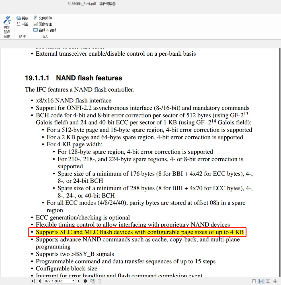
And I found this limitation in the B4860RM_RevI. Can it confirm that this 8kb-pagesize chip is not supported?
This is the limitation to support 8K page size NAND flash.
