
- NXP Forums
- Product Forums
- General Purpose MicrocontrollersGeneral Purpose Microcontrollers
- i.MX Forumsi.MX Forums
- QorIQ Processing PlatformsQorIQ Processing Platforms
- Identification and SecurityIdentification and Security
- Power ManagementPower Management
- MCX Microcontrollers
- S32G
- S32K
- S32V
- MPC5xxx
- Other NXP Products
- Wireless Connectivity
- S12 / MagniV Microcontrollers
- Powertrain and Electrification Analog Drivers
- Sensors
- Vybrid Processors
- Digital Signal Controllers
- 8-bit Microcontrollers
- ColdFire/68K Microcontrollers and Processors
- PowerQUICC Processors
- OSBDM and TBDML
-
- Solution Forums
- Software Forums
- MCUXpresso Software and ToolsMCUXpresso Software and Tools
- CodeWarriorCodeWarrior
- MQX Software SolutionsMQX Software Solutions
- Model-Based Design Toolbox (MBDT)Model-Based Design Toolbox (MBDT)
- FreeMASTER
- eIQ Machine Learning Software
- Embedded Software and Tools Clinic
- S32 SDK
- S32 Design Studio
- Vigiles
- GUI Guider
- Zephyr Project
- Voice Technology
- Application Software Packs
- Secure Provisioning SDK (SPSDK)
- Processor Expert Software
-
- Topics
- Mobile Robotics - Drones and RoversMobile Robotics - Drones and Rovers
- NXP Training ContentNXP Training Content
- University ProgramsUniversity Programs
- Rapid IoT
- NXP Designs
- SafeAssure-Community
- OSS Security & Maintenance
- Using Our Community
-
- Cloud Lab Forums
-
- Home
- :
- 製品フォーラム
- :
- PowerQUICCプロセッサ
- :
- local memory Map for MPC8358E processor
local memory Map for MPC8358E processor
- RSS フィードを購読する
- トピックを新着としてマーク
- トピックを既読としてマーク
- このトピックを現在のユーザーにフロートします
- ブックマーク
- 購読
- ミュート
- 印刷用ページ
- 新着としてマーク
- ブックマーク
- 購読
- ミュート
- RSS フィードを購読する
- ハイライト
- 印刷
- 不適切なコンテンツを報告
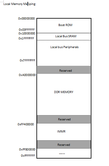
Hi Folks
We are using MPC8358E processor and we configured the local memory as shown in the fig.. mainly we are struggling with DDR interface. so please confirm this memory mapping.
is this DDR memory mapping is right?

Regards,
Venkat
解決済! 解決策の投稿を見る。
- 新着としてマーク
- ブックマーク
- 購読
- ミュート
- RSS フィードを購読する
- ハイライト
- 印刷
- 不適切なコンテンツを報告
Please refer to the MPC8360E PowerQUICC II Pro Integrated Communications Processor Family Reference Manual, 4.4.3 System Clock Domains:
"The internal ddr_clk frequency (for DDR) is determined by RCWL[DDRCM]. Note that the lb_clk clock
frequency (for Secondary DDR) is determined by RCWL[LBCM]. See Section 4.3.2.1, “Reset
Configuration Word Low Register (RCWLR).” Note that ddr_clk is not the external memory bus
frequency; ddr_clk passes through the DDR clock divider (÷2) to create the differential DDR memory bus
clock outputs (MCK and MCK). However, the data rate is the same frequency as ddr_clk."
- 新着としてマーク
- ブックマーク
- 購読
- ミュート
- RSS フィードを購読する
- ハイライト
- 印刷
- 不適切なコンテンツを報告
Proposed memory map is incorrect.
Please read the MPC8360E PowerQUICC II Pro Integrated Communications Processor Family Reference Manual, 5.2 Local Memory Map Overview and Example
- 新着としてマーク
- ブックマーク
- 購読
- ミュート
- RSS フィードを購読する
- ハイライト
- 印刷
- 不適切なコンテンツを報告
Thank you for replying,
As per MPC8360E PowerQUICC II Pro Integrated Communications Processor Family Reference Manual says, we can put boot flash on All zeros address or 0xFF80_0000 address. can you please elaborate more on this?. so that, my memory mapping is incorrect...
Regards,
Venkat
- 新着としてマーク
- ブックマーク
- 購読
- ミュート
- RSS フィードを購読する
- ハイライト
- 印刷
- 不適切なコンテンツを報告
What is the DDR SDRAM size?
- 新着としてマーク
- ブックマーク
- 購読
- ミュート
- RSS フィードを購読する
- ハイライト
- 印刷
- 不適切なコンテンツを報告
DDR size-64MB
Manfr- micron
- 新着としてマーク
- ブックマーク
- 購読
- ミュート
- RSS フィードを購読する
- ハイライト
- 印刷
- 不適切なコンテンツを報告
What are RCWLR and RCWHR values?
You wrote:
> we are struggling with DDR interface
What does it mean?
- 新着としてマーク
- ブックマーク
- 購読
- ミュート
- RSS フィードを購読する
- ハイライト
- 印刷
- 不適切なコンテンツを報告
RCWLR- 0x02230086
RCWHR- 0x00600000
- 新着としてマーク
- ブックマーク
- 購読
- ミュート
- RSS フィードを購読する
- ハイライト
- 印刷
- 不適切なコンテンツを報告
You wrote:
> we are struggling with DDR interface
What does it mean?
- 新着としてマーク
- ブックマーク
- 購読
- ミュート
- RSS フィードを購読する
- ハイライト
- 印刷
- 不適切なコンテンツを報告
#RCWLR Value :- 0x02230086
#LBCM-0 LBCM is equal to csb clk (266MHz)
#DDRCM-0 DDRCM is equal to csb clk (266MHz)
#SVCOD-00 system PLL VCO division is 4
#SPMF - 0010 system PLL multiplication factor is 2:1
#COREPLL -0100011 Core freq. 1600MHZ
#CEVCOD -10 QUIIC engine Freq. is 800MHZ
#CEPDF - 0 QUIIC Engine PLL div. factor is 0
#CEPMF- 00110 QUICC engine PLL mortification factor 6
#RCWHR Value :- 0x00600000
#PCIHOST-0 PCI is disable (not using)
#PCIARB-0 PCI arbiter is disable
#PCICKDRV - 0 PCI Buffers are disable
#COEDIS- 0 core can boot without waiting for config. by external master
#BMS- 0 boot memory space is all zeros to 0x007f_ffff
#BOOTSEQ- 00 boot sequencer disabled
#SWEN - 0 Software WDT disable
#ROMLOC- 110 local bus GPCM 16-bit ROM
#SDDRIOE -0 secondary DDR I/O disable
#TLE -0 big-endian mode
#LALE - 0 normal LALE timing
#LDP-0 initial value of SCIRL[LDP_A] is 1 means that LDP0-LDP3 are used for local data parity
- 新着としてマーク
- ブックマーク
- 購読
- ミュート
- RSS フィードを購読する
- ハイライト
- 印刷
- 不適切なコンテンツを報告
- 新着としてマーク
- ブックマーク
- 購読
- ミュート
- RSS フィードを購読する
- ハイライト
- 印刷
- 不適切なコンテンツを報告
You wrote:
> we are struggling with DDR interface
What does it mean?
- 新着としてマーク
- ブックマーク
- 購読
- ミュート
- RSS フィードを購読する
- ハイライト
- 印刷
- 不適切なコンテンツを報告
> we are struggling with DDR interface
>What does it mean?
I am not able to access DDR memory. and DDR doesn't responding to the configured address.
- 新着としてマーク
- ブックマーク
- 購読
- ミュート
- RSS フィードを購読する
- ハイライト
- 印刷
- 不適切なコンテンツを報告
There are two possibilities:
1) DDR SDRAM connection is incorrect
2) DDR controller initialization settings are incorrect.
- 新着としてマーク
- ブックマーク
- 購読
- ミュート
- RSS フィードを購読する
- ハイライト
- 印刷
- 不適切なコンテンツを報告
- 新着としてマーク
- ブックマーク
- 購読
- ミュート
- RSS フィードを購読する
- ハイライト
- 印刷
- 不適切なコンテンツを報告
Please provide:
1) DDR SDRAM connection schematics as searchable PDF
2) what is measured frequency of the MCK?
- 新着としてマーク
- ブックマーク
- 購読
- ミュート
- RSS フィードを購読する
- ハイライト
- 印刷
- 不適切なコンテンツを報告
- 新着としてマーク
- ブックマーク
- 購読
- ミュート
- RSS フィードを購読する
- ハイライト
- 印刷
- 不適切なコンテンツを報告
@ufedor are u there?
- 新着としてマーク
- ブックマーク
- 購読
- ミュート
- RSS フィードを購読する
- ハイライト
- 印刷
- 不適切なコンテンツを報告
sir,
can we control DDR operating frequecy(MCK)? if it is yes! How?
- 新着としてマーク
- ブックマーク
- 購読
- ミュート
- RSS フィードを購読する
- ハイライト
- 印刷
- 不適切なコンテンツを報告
Please refer to the MPC8360E PowerQUICC II Pro Integrated Communications Processor Family Reference Manual, 4.4.3 System Clock Domains:
"The internal ddr_clk frequency (for DDR) is determined by RCWL[DDRCM]. Note that the lb_clk clock
frequency (for Secondary DDR) is determined by RCWL[LBCM]. See Section 4.3.2.1, “Reset
Configuration Word Low Register (RCWLR).” Note that ddr_clk is not the external memory bus
frequency; ddr_clk passes through the DDR clock divider (÷2) to create the differential DDR memory bus
clock outputs (MCK and MCK). However, the data rate is the same frequency as ddr_clk."