- Forums
- Product Forums
- General Purpose MicrocontrollersGeneral Purpose Microcontrollers
- i.MX Forumsi.MX Forums
- QorIQ Processing PlatformsQorIQ Processing Platforms
- Identification and SecurityIdentification and Security
- Power ManagementPower Management
- Wireless ConnectivityWireless Connectivity
- RFID / NFCRFID / NFC
- Advanced AnalogAdvanced Analog
- MCX Microcontrollers
- S32G
- S32K
- S32V
- MPC5xxx
- Other NXP Products
- S12 / MagniV Microcontrollers
- Powertrain and Electrification Analog Drivers
- Sensors
- Vybrid Processors
- Digital Signal Controllers
- 8-bit Microcontrollers
- ColdFire/68K Microcontrollers and Processors
- PowerQUICC Processors
- OSBDM and TBDML
- S32M
- S32Z/E
-
- Solution Forums
- Software Forums
- MCUXpresso Software and ToolsMCUXpresso Software and Tools
- CodeWarriorCodeWarrior
- MQX Software SolutionsMQX Software Solutions
- Model-Based Design Toolbox (MBDT)Model-Based Design Toolbox (MBDT)
- FreeMASTER
- eIQ Machine Learning Software
- Embedded Software and Tools Clinic
- S32 SDK
- S32 Design Studio
- GUI Guider
- Zephyr Project
- Voice Technology
- Application Software Packs
- Secure Provisioning SDK (SPSDK)
- Processor Expert Software
- Generative AI & LLMs
-
- Topics
- Mobile Robotics - Drones and RoversMobile Robotics - Drones and Rovers
- NXP Training ContentNXP Training Content
- University ProgramsUniversity Programs
- Rapid IoT
- NXP Designs
- SafeAssure-Community
- OSS Security & Maintenance
- Using Our Community
-
- Cloud Lab Forums
-
- Knowledge Bases
- ARM Microcontrollers
- i.MX Processors
- Identification and Security
- Model-Based Design Toolbox (MBDT)
- QorIQ Processing Platforms
- S32 Automotive Processing Platform
- Wireless Connectivity
- CodeWarrior
- MCUXpresso Suite of Software and Tools
- MQX Software Solutions
- RFID / NFC
- Advanced Analog
-
- NXP Tech Blogs
- Home
- :
- RFID / NFC
- :
- NFC
- :
- CRLC663: general purpose output functionality
CRLC663: general purpose output functionality
- RSS フィードを購読する
- トピックを新着としてマーク
- トピックを既読としてマーク
- このトピックを現在のユーザーにフロートします
- ブックマーク
- 購読
- ミュート
- 印刷用ページ
CRLC663: general purpose output functionality
- 新着としてマーク
- ブックマーク
- 購読
- ミュート
- RSS フィードを購読する
- ハイライト
- 印刷
- 不適切なコンテンツを報告
Hi,
We would like to make use of the additional general purpose outputs of the CRLC663 chip in a future project to save pins on a MCU. We would like to use the Pins OUT0 to OUT3 which are usually for the boundary scan.
I've not found any information about the hardware functionality of the pins in the datasheet. The critical informations would be if the pins are either "voltage out" (like a MCU) or "sink" (eg. open drain) and how much current can be used per pin and in common. I know that some devices can provide like 5mA per port, but for example only 15mA in sum of all pins.
We aim to use 4 LED's which have 1-3mA per LED.
Also it would be interesting how the outputs react when the device is in reset or sleep mode.
Thank you for any information.
- 新着としてマーク
- ブックマーク
- 購読
- ミュート
- RSS フィードを購読する
- ハイライト
- 印刷
- 不適切なコンテンツを報告
Hello Jonathan ,
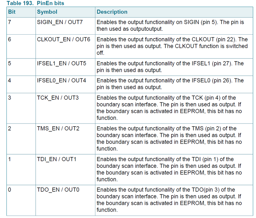
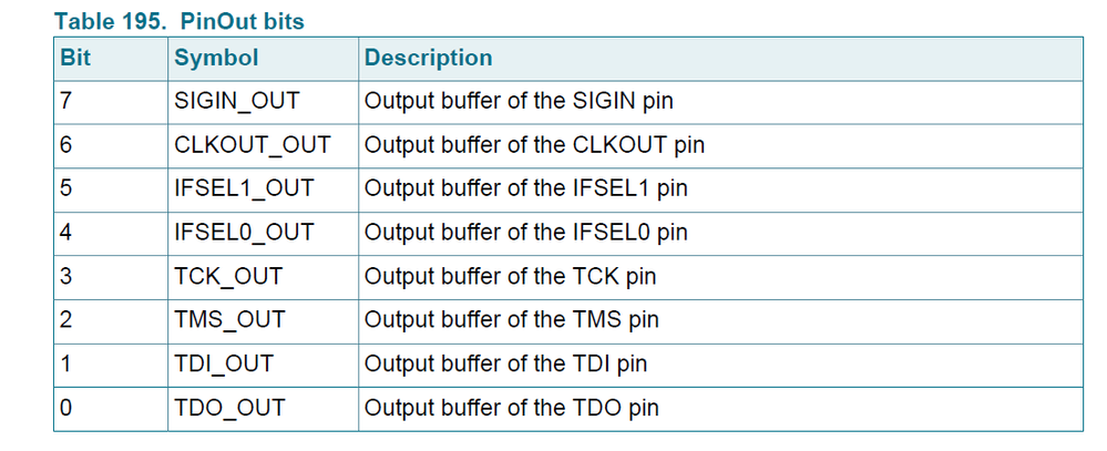
OUT0~OUT7 all can be used as GPIO function. But these pins are multiplexed. You should do 2 steps for GPIO:
1. Enable them on corresponding bit in Register "PinEn"
[note]
You can try to write 1 at bit0, and check if GPO function is enabled, otherwise write 0, please! I also didn't find detailed description on 1 or 0 for GPO function.
2. Output High Or Low in Register "8.15.2 PinOut"
Write 1 on related bit, High level should be output, otherwise Low level.
In addtion, if your LED needs 1-3mA, it is no problem to driver them diretly via GPO. if higher current is needed, you can add a MOSFET to driver LEDs.
Have a nice day!
Best Regards,
Weidong Sun


