- Forums
- Product Forums
- General Purpose MicrocontrollersGeneral Purpose Microcontrollers
- i.MX Forumsi.MX Forums
- QorIQ Processing PlatformsQorIQ Processing Platforms
- Identification and SecurityIdentification and Security
- Power ManagementPower Management
- Wireless ConnectivityWireless Connectivity
- RFID / NFCRFID / NFC
- MCX Microcontrollers
- S32G
- S32K
- S32V
- MPC5xxx
- Other NXP Products
- S12 / MagniV Microcontrollers
- Powertrain and Electrification Analog Drivers
- Sensors
- Vybrid Processors
- Digital Signal Controllers
- 8-bit Microcontrollers
- ColdFire/68K Microcontrollers and Processors
- PowerQUICC Processors
- OSBDM and TBDML
- S32M
-
- Solution Forums
- Software Forums
- MCUXpresso Software and ToolsMCUXpresso Software and Tools
- CodeWarriorCodeWarrior
- MQX Software SolutionsMQX Software Solutions
- Model-Based Design Toolbox (MBDT)Model-Based Design Toolbox (MBDT)
- FreeMASTER
- eIQ Machine Learning Software
- Embedded Software and Tools Clinic
- S32 SDK
- S32 Design Studio
- GUI Guider
- Zephyr Project
- Voice Technology
- Application Software Packs
- Secure Provisioning SDK (SPSDK)
- Processor Expert Software
-
- Topics
- Mobile Robotics - Drones and RoversMobile Robotics - Drones and Rovers
- NXP Training ContentNXP Training Content
- University ProgramsUniversity Programs
- Rapid IoT
- NXP Designs
- SafeAssure-Community
- OSS Security & Maintenance
- Using Our Community
-
- Cloud Lab Forums
-
- Knowledge Bases
- ARM Microcontrollers
- i.MX Processors
- Identification and Security
- Model-Based Design Toolbox (MBDT)
- QorIQ Processing Platforms
- S32 Automotive Processing Platform
- Wireless Connectivity
- CodeWarrior
- MCUXpresso Suite of Software and Tools
- MQX Software Solutions
-
- Home
- :
- Product Forums
- :
- MPC5xxx
- :
- Re: how to configure spi for communicating W25N01GVxxIG/IT from mpc5748g
how to configure spi for communicating W25N01GVxxIG/IT from mpc5748g
- Subscribe to RSS Feed
- Mark Topic as New
- Mark Topic as Read
- Float this Topic for Current User
- Bookmark
- Subscribe
- Mute
- Printer Friendly Page
how to configure spi for communicating W25N01GVxxIG/IT from mpc5748g
- Mark as New
- Bookmark
- Subscribe
- Mute
- Subscribe to RSS Feed
- Permalink
- Report Inappropriate Content
I want to configure spi for communicating with an external NAND Flash module from MPC5748G mcu. Suppose I am transmitting 0x9F opcode from MCU to Flash via spi, then flash module will respond after 8 dummy clocks as per the design. Please see the screenshot for better understanding. Now after transmitting the data, in the receive buffer, the content is showing null. MCU is unable to get any data. Status is showing success. What could be the error over here??
If anyone have any SPI sample code for mpc5748g, please share it.
- Mark as New
- Bookmark
- Subscribe
- Mute
- Subscribe to RSS Feed
- Permalink
- Report Inappropriate Content
If this is communication protocol on connected slave device, then you CPU side (master), you will need to transmit 5 bytes: 0x9F plus 4 times dummy bytes. Are you doing it like that?
Another point what is needed to check is HW connection of connected device, typically some external pull resistors are needed for correct functionality.
- Mark as New
- Bookmark
- Subscribe
- Mute
- Subscribe to RSS Feed
- Permalink
- Report Inappropriate Content
In the hardware 33ohm pull up resistors are using. I guess that is enough. Please correct if its wrong..
- Mark as New
- Bookmark
- Subscribe
- Mute
- Subscribe to RSS Feed
- Permalink
- Report Inappropriate Content
Yes I am transmitting four more bytes after transmitting 0x9f.
for eg:
spi_tx(0x9f);
spi_tx(0xa5);
spi_tx(0xa5);
spi_tx(0xa5);
spi_tx(0xa5);
Let me know if its the correct way to transmit.
Also, what is the value of dummy bytes? I am transmitting 0xA5 as dummy data. Is there any specific value to be transmitted?
- Mark as New
- Bookmark
- Subscribe
- Mute
- Subscribe to RSS Feed
- Permalink
- Report Inappropriate Content
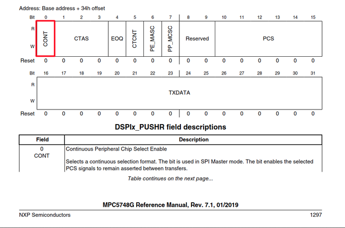
I don't know what's the driver but in principle you can send any value for dummy bytes. Command need to keep CS asserted between data words - this can be achieved by setting CONT bit for all these words, excluding last one.
- Mark as New
- Bookmark
- Subscribe
- Mute
- Subscribe to RSS Feed
- Permalink
- Report Inappropriate Content
Thanks for the help. Here, the processor selected in S32DS is MPC5748G_176 and driver generated for added spi component is dspi_driver.c. I will attach the spi_driver file over here. Thanks for pointing out that CS should be selected through out transmission. But how to set the CONT bit ?
- Mark as New
- Bookmark
- Subscribe
- Mute
- Subscribe to RSS Feed
- Permalink
- Report Inappropriate Content
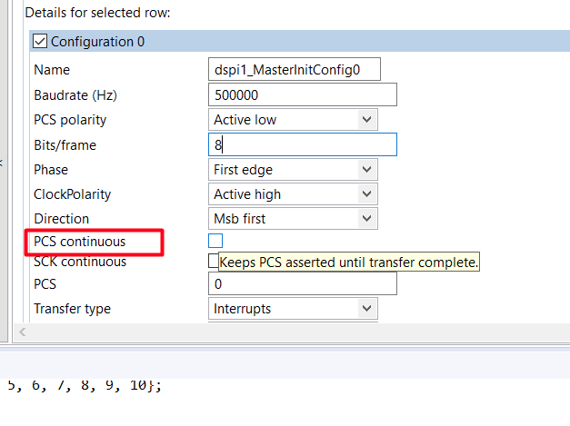
Apparently it is possible to set-up in processor expert configration:
- Mark as New
- Bookmark
- Subscribe
- Mute
- Subscribe to RSS Feed
- Permalink
- Report Inappropriate Content
Continuous SS was already checked in the component inspector window of spi. Still it was not working. Other than calling spi_init() function, do I need to perform any other task prior to the transmission of data via spi, in case of w25n01xx NAND Flash module. For example do I need to perform any reset or disabling write protection etc..
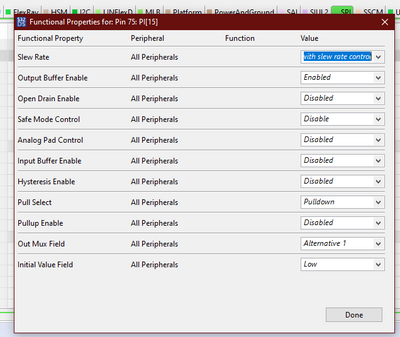
This is the functional properties of chip select pin. Do i need to modify any properties with respect to chip select pin? Also for MOSI & MISO pins do I need to modify any properties?
- Mark as New
- Bookmark
- Subscribe
- Mute
- Subscribe to RSS Feed
- Permalink
- Report Inappropriate Content
I have checked example code dspi_master_mpc5748g and mentioned setting does affect CONT bit.
Have you measured with scope to check whether transmitted waveforms fit to communication protocol described in the datasheet of connected device? It is currently what I recommend to do to analyze root cause of the issue.
- Mark as New
- Bookmark
- Subscribe
- Mute
- Subscribe to RSS Feed
- Permalink
- Report Inappropriate Content
In the datasheet of winbond w25n01xx NAND Flash, below shown is mentioned for spi configuration. I think i have configured spi by taking that into account. Please correct me, if I am wrong.
DATASHEET NOTE
Standard SPI instructions use the DI input pin to serially write instructions, addresses or data to the device on the rising edge of CLK. The DO output pin is used to read data or status from the device on the falling edge of CLK.
SPI bus operation Mode 0 (0,0) and 3 (1,1) are supported. The primary difference between Mode 0 and
Mode 3 concerns the normal state of the CLK signal when the SPI bus master is in standby and data is not being transferred to the Serial Flash. For Mode 0, the CLK signal is normally low on the falling and rising edges of /CS. For Mode 3, the CLK signal is normally high on the falling and rising edges of /CS.
SPI CONFIGURATION
const spi_master_t spi1_MasterConfig0 =
{
.baudRate = 100000,
.ssPolarity = SPI_ACTIVE_LOW,
.continuousSS = true,
.frameSize = 8,
.clockPhase = READ_ON_EVEN_EDGE,
.clockPolarity = SPI_ACTIVE_LOW,
.bitOrder = SPI_TRANSFER_MSB_FIRST,
.transferType = SPI_USING_INTERRUPTS,
.rxDMAChannel = 255U,
.txDMAChannel = 255U,
.callback = NULL,
.callbackParam = NULL,
.ssPin = 0,
.extension = NULL
};
__________
- Mark as New
- Bookmark
- Subscribe
- Mute
- Subscribe to RSS Feed
- Permalink
- Report Inappropriate Content
I am sorry, I am afraid I don't understand your comment. The note says that your spi slave device support both clocking modes - continuous and non-continuous - but it is not related to CONT bit as discussed above.
- Mark as New
- Bookmark
- Subscribe
- Mute
- Subscribe to RSS Feed
- Permalink
- Report Inappropriate Content
For NAND FLASH, in MOSI, CS and clk lines the fall time and rise time needs to be <5ns. But currently when measured, the rise time is 12ns and fall time is 22ns. The master is MPC5748G and the slave is NAND Flash w25n01gv. So, from the MCU software side, is there any way to reduce the fall & rise time time for these output lines of spi.
- Mark as New
- Bookmark
- Subscribe
- Mute
- Subscribe to RSS Feed
- Permalink
- Report Inappropriate Content
You can configure slew rate control bits for specified pads. By default 00 option (slowest edges) is choosen.
- Mark as New
- Bookmark
- Subscribe
- Mute
- Subscribe to RSS Feed
- Permalink
- Report Inappropriate Content
Thank you so much.. That was really helpful. Now I am getting response. In oscilloscope, when MISO line is captured, the data is there and its the correct response also. But that data is not updated in received buffer in the spi function.
SPI_MasterTransferBlocking(&spi1Instance, &tx_buffer, &rx_buffer, 1, 100);
while(STATUS_SUCCESS != SPI_GetStatus(&spi1Instance));
return rx_buffer;
always this receiver buffer is always empty.
Please help me to resolve it.
It seems like in POPR register, no data is loaded, But data is there in MISO line when checked using oscilloscope. What could be the reason for this?
- Mark as New
- Bookmark
- Subscribe
- Mute
- Subscribe to RSS Feed
- Permalink
- Report Inappropriate Content
It seems like in POPR register, no data is loaded, But data is there in MISO line when checked using oscilloscope. What could be the reason for this?
- Mark as New
- Bookmark
- Subscribe
- Mute
- Subscribe to RSS Feed
- Permalink
- Report Inappropriate Content
Do you have properly setup SIU configuration for input pins?
- Mark as New
- Bookmark
- Subscribe
- Mute
- Subscribe to RSS Feed
- Permalink
- Report Inappropriate Content
I guess MSCR and IMCR is configured in the right way. MSCR[SSS] is 00000010, so input mux[0] is assigned value 2 and input_mux_reg[0] is assigned 300. input mux_1 to 7 are disabled. Also for the SPI input pin of MCU, HYSTERESYS, pull select and open drain are disabled. Do i need to modify any of these to receive data properly. If i am wrong, please do correct me.
- Mark as New
- Bookmark
- Subscribe
- Mute
- Subscribe to RSS Feed
- Permalink
- Report Inappropriate Content
Could you explicitly specify IMCR and MSCR numbers and their values? Thanks
- Mark as New
- Bookmark
- Subscribe
- Mute
- Subscribe to RSS Feed
- Permalink
- Report Inappropriate Content
SIUL_GPIO_PIN PI[14], pinPortIdx 142u, IMCR 300, MSCR[SSS]=00000010 (0X02)
PORT_MUX_AS_GPIO
PORT_OUTPUT_BUFFER_DISABLED,
PORT_OPEN_DRAIN_DISABLED,
HALF_STRENGTH_WITH_SLEWRATE_CONTROL,
PORT_HYSTERESYS_DISABLED,
PORT_SAFE_MODE_DISABLED,
PORT_ANALOG_PAD_CONTROL_DISABLED,
PORT_INPUT_BUFFER_ENABLED,
PORT_INTERNAL_PULL_NOT_ENABLED,
input_mux_reg[0]=300
input_mux[0]=0x02
- Mark as New
- Bookmark
- Subscribe
- Mute
- Subscribe to RSS Feed
- Permalink
- Report Inappropriate Content
If I understand you description right (what I am not sure) I think you have it configured incorrectly. You have to have configured 2 registers MSCR142 (to enable input buffer) and IMCR300 (i.e. MSCR812 in order to route pin to module input.
- Mark as New
- Bookmark
- Subscribe
- Mute
- Subscribe to RSS Feed
- Permalink
- Report Inappropriate Content
Already MSCR[142] and IMCR[300] are configured and in MSCR[142] register I have enabled input buffer and IMCR[300] have sss bit and its value is 2.


