- Forums
- Product Forums
- General Purpose MicrocontrollersGeneral Purpose Microcontrollers
- i.MX Forumsi.MX Forums
- QorIQ Processing PlatformsQorIQ Processing Platforms
- Identification and SecurityIdentification and Security
- Power ManagementPower Management
- MCX Microcontrollers
- S32G
- S32K
- S32V
- MPC5xxx
- Other NXP Products
- Wireless Connectivity
- S12 / MagniV Microcontrollers
- Powertrain and Electrification Analog Drivers
- Sensors
- Vybrid Processors
- Digital Signal Controllers
- 8-bit Microcontrollers
- ColdFire/68K Microcontrollers and Processors
- PowerQUICC Processors
- OSBDM and TBDML
- S32M
-
- Solution Forums
- Software Forums
- MCUXpresso Software and ToolsMCUXpresso Software and Tools
- CodeWarriorCodeWarrior
- MQX Software SolutionsMQX Software Solutions
- Model-Based Design Toolbox (MBDT)Model-Based Design Toolbox (MBDT)
- FreeMASTER
- eIQ Machine Learning Software
- Embedded Software and Tools Clinic
- S32 SDK
- S32 Design Studio
- GUI Guider
- Zephyr Project
- Voice Technology
- Application Software Packs
- Secure Provisioning SDK (SPSDK)
- Processor Expert Software
- MCUXpresso Training Hub
-
- Topics
- Mobile Robotics - Drones and RoversMobile Robotics - Drones and Rovers
- NXP Training ContentNXP Training Content
- University ProgramsUniversity Programs
- Rapid IoT
- NXP Designs
- SafeAssure-Community
- OSS Security & Maintenance
- Using Our Community
-
- Cloud Lab Forums
-
- Knowledge Bases
- ARM Microcontrollers
- i.MX Processors
- Identification and Security
- Model-Based Design Toolbox (MBDT)
- QorIQ Processing Platforms
- S32 Automotive Processing Platform
- Wireless Connectivity
- CodeWarrior
- MCUXpresso Suite of Software and Tools
- MQX Software Solutions
-
- Home
- :
- 汎用マイクロコントローラ
- :
- LPCマイクロコントローラ
- :
- Flash pages and sectors on the LPC55S69
Flash pages and sectors on the LPC55S69
- RSS フィードを購読する
- トピックを新着としてマーク
- トピックを既読としてマーク
- このトピックを現在のユーザーにフロートします
- ブックマーク
- 購読
- ミュート
- 印刷用ページ
Flash pages and sectors on the LPC55S69
- 新着としてマーク
- ブックマーク
- 購読
- ミュート
- RSS フィードを購読する
- ハイライト
- 印刷
- 不適切なコンテンツを報告
The terminology in the documentation for the LPC55S69's flash API and the MCUX driver is inconsistent and not well defined. What I'm trying to determine is the block size for erase and page program.
The driver itself reports a page size of 512 bytes and a sector size of 32768. For most NOR flash vendors I've used, erase operations are performed on full sectors and program operations are performed on pages. The FLASH_Erase() description says: "This function erases the appropriate number of flash sectors based on the desired start address and length."
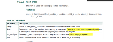
To me that implies that it has to erase at least 1 sector, which would be 32k. That's not supported by other mentions in the docs, though, like the lengthInBytes parameter: "The length, given in bytes (not words or long-words) to be erased. Must be 512bytes-aligned."
This seems to say that 512-byte erases are possible. Can someone confirm that this is true? If so, what is the significance of the sector size? There's also a block size which seems to be the same as the total size.
Also, it's not relevant to the bootloader I'm working on today, but what is the minimum size that can be written, and its alignment? The driver says the length must be 512-byte aligned (I think that is trying to say that it needs to be a multiple of 512 bytes, not that the value needs to be aligned on a 512-byte boundary) but the user's manual suggests that 128 bits is the minimum write size. Can someone clarify that? It's useful to be able to perform many small writes to a previously-erased page to reduce the wear on the flash when updating values.
Thanks,
Scott
- 新着としてマーク
- ブックマーク
- 購読
- ミュート
- RSS フィードを購読する
- ハイライト
- 印刷
- 不適切なコンテンツを報告
Hello @scottm
1, "The driver says the length must be 512-byte aligned (I think that is trying to say that it needs to be a multiple of 512 bytes,)"
->> Yes, the minimum size of program is one page (512 bytes), and can be multiple of 512 bytes.
2, "but the user's manual suggests that 128 bits is the minimum write size."
->> Could you please share me where mentioned this, i will help to check.
3, The minimum size of erase also is one page:
BR
Alice
- 新着としてマーク
- ブックマーク
- 購読
- ミュート
- RSS フィードを購読する
- ハイライト
- 印刷
- 不適切なコンテンツを報告
Hi Alice,
The part that has me confused is this:
For writing, a number of APB writes are needed to fully define a memory word, which is
larger than 32 bits. The controller accumulates data inside its own internal storage, until
the content of a full memory word has been specified. When this is done, the full word is
transferred to the memory’s page register (at the position specified by the STARTA
register), as a single operation.
Data to be written is accumulated inside the controller’s DATAW0-DATAW3 registers.
After specifying an address in the STARTA register and 128 bit of data in the DATAW0-3
registers, it’s possible to activate the controller’s Write” command, which will transfer the
data to the memory’s page register, at the position indicated by the STARTA register (only
the column part of the address is significant).
The sections on flash and particularly on the ROM functions are noticeably less well-written (and edited) than the rest of the manual. It's a bit of a jumble.
One issue is that it repeatedly mentions the column part of the address, without specifying how many bits make up the column part.
Scott
- 新着としてマーク
- ブックマーク
- 購読
- ミュート
- RSS フィードを購読する
- ハイライト
- 印刷
- 不適切なコンテンツを報告
Hello @scottm
This part is about how to use register control flash, recommend directly use Flash APIs.
BR
Alice
