- Forums
- Product Forums
- General Purpose MicrocontrollersGeneral Purpose Microcontrollers
- i.MX Forumsi.MX Forums
- QorIQ Processing PlatformsQorIQ Processing Platforms
- Identification and SecurityIdentification and Security
- Power ManagementPower Management
- MCX Microcontrollers
- S32G
- S32K
- S32V
- MPC5xxx
- Other NXP Products
- Wireless Connectivity
- S12 / MagniV Microcontrollers
- Powertrain and Electrification Analog Drivers
- Sensors
- Vybrid Processors
- Digital Signal Controllers
- 8-bit Microcontrollers
- ColdFire/68K Microcontrollers and Processors
- PowerQUICC Processors
- OSBDM and TBDML
- S32M
-
- Solution Forums
- Software Forums
- MCUXpresso Software and ToolsMCUXpresso Software and Tools
- CodeWarriorCodeWarrior
- MQX Software SolutionsMQX Software Solutions
- Model-Based Design Toolbox (MBDT)Model-Based Design Toolbox (MBDT)
- FreeMASTER
- eIQ Machine Learning Software
- Embedded Software and Tools Clinic
- S32 SDK
- S32 Design Studio
- GUI Guider
- Zephyr Project
- Voice Technology
- Application Software Packs
- Secure Provisioning SDK (SPSDK)
- Processor Expert Software
- MCUXpresso Training Hub
-
- Topics
- Mobile Robotics - Drones and RoversMobile Robotics - Drones and Rovers
- NXP Training ContentNXP Training Content
- University ProgramsUniversity Programs
- Rapid IoT
- NXP Designs
- SafeAssure-Community
- OSS Security & Maintenance
- Using Our Community
-
- Cloud Lab Forums
-
- Knowledge Bases
- ARM Microcontrollers
- i.MX Processors
- Identification and Security
- Model-Based Design Toolbox (MBDT)
- QorIQ Processing Platforms
- S32 Automotive Processing Platform
- Wireless Connectivity
- CodeWarrior
- MCUXpresso Suite of Software and Tools
- MQX Software Solutions
-
- Home
- :
- 通用微控制器
- :
- Kinetis微控制器
- :
- K66 Clock Generation
K66 Clock Generation
Hello,
I am using K66 controller MK66FX1M0VLQ18 . I want run at high speed of 180Mhz and write/read from the flash. I am not getting which all registers to configure. Please help me out
已解决! 转到解答。
Hi
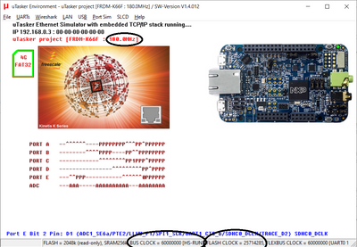
Use the uTasker open source project as reference - https://github.com/uTasker/uTasker-Kinetis select FRDM_K66F and enable USE_HIGH_SPEED_RUN_MODE and it will generate you a project that runs at full speed and its simulator will show you the details and allow you to step the code (in Visual Studio) to see all steps needed.
Also follow https://www.utasker.com/kinetis/MCG.html which gives some practical insights into the workings of the MCG.
Beware that the high speed run mode is required to operate at 180MHz and flash programming is not possible in this mode. Ether you need to switch clocks to <= 120MHz and move to RUN mode each time programming is required or else you need to generally use RUN mode (limited to 120MHz).
The actual clock configuration for max. speed on all buses for the K66 (assuming 12MHz crystal source) is:
#define CLOCK_DIV 1
#define CLOCK_MUL 30                                                     // (((12 /1) * 30) / 2)) gives 128MHz
#define SYSTEM_CLOCK_DIVIDE 1                                            // 180MHz system clock
#define BUS_CLOCK_DIVIDE     3                                           // 180/3 to give 60MHz (max. 60MHz)
#define FLEX_CLOCK_DIVIDE    3                                           // 180/3 to give 60MHz (max. 60MHz)
#define FLASH_CLOCK_DIVIDE   7                                           // 180/7 to give 25.714MHz (max. 28MHz)

    MCG_C2 = (MCG_C2_RANGE_8M_32M | MCG_C2_EREFS | MCG_C2_LOCRE0);       // select crystal oscillator and select a suitable range
    MCG_C1 = (MCG_C1_CLKS_EXTERN_CLK | MCG_C1_FRDIV_32);                 // switch to external source (the FLL input clock is set to as close to its input range as possible, although this is not absolutely necessary if the FLL will not be used)
    _WAIT_REGISTER_FALSE(MCG_S, MCG_S_OSCINIT);                          // loop until the crystal source has been selected
    _WAIT_REGISTER_TRUE(MCG_S, MCG_S_IREFST);                            // loop until the FLL source is no longer the internal reference clock
    while ((MCG_S & MCG_S_CLKST_MASK) != MCG_S_CLKST_EXTERN_CLK) {}      // loop until the external reference clock source is valid
    MCG_C5 = ((CLOCK_DIV - 1) | MCG_C5_PLLSTEN0);                        // now move from state FEE to state PBE (or FBE) PLL remains enabled in normal stop modes
    MCG_C6 = ((CLOCK_MUL - MCG_C6_VDIV0_LOWEST) | MCG_C6_PLLS);          // set the PLL multiplication factor
    while ((MCG_S & MCG_S_PLLST) == 0) {}                                // loop until the PLLS clock source becomes valid
    while ((MCG_S & MCG_S_LOCK) == 0) {}                                 // loop until PLL locks
    SIM_CLKDIV1 = (((SYSTEM_CLOCK_DIVIDE - 1) << 28) | ((BUS_CLOCK_DIVIDE - 1) << 24) | ((FLEX_CLOCK_DIVIDE - 1) << 20) | ((FLASH_CLOCK_DIVIDE - 1) << 16)); // prepare bus clock divides
    SMC_PMCTRL = SMC_PMCTRL_RUNM_HSRUN;                                  // set high speed run mode (restrictions apply) so that the clock speeds can be obtained
    MCG_C1 = (MCG_C1_CLKS_PLL_FLL | MCG_C1_FRDIV_1024);                  // finally move from PBE to PEE mode - switch to PLL clock
    while ((MCG_S & MCG_S_CLKST_MASK) != MCG_S_CLKST_PLL) {}             // loop until the PLL clock is selected
    SIM_CLKDIV3 = PERIPHERAL_CLOCK_DIVIDE_VALUE;                         // configure the optional peripheral clock divide early since it shouldn't be changed once LPUARTs or TPU have started using it
Simulation of the operation:
Regards
Mark
[uTasker project developer for Kinetis and i.MX RT]
Contact me by personal message or on the uTasker web site to discuss professional training, solutions to problems or product development requirements
