- Forums
- Product Forums
- General Purpose MicrocontrollersGeneral Purpose Microcontrollers
- i.MX Forumsi.MX Forums
- QorIQ Processing PlatformsQorIQ Processing Platforms
- Identification and SecurityIdentification and Security
- Power ManagementPower Management
- MCX Microcontrollers
- S32G
- S32K
- S32V
- MPC5xxx
- Other NXP Products
- Wireless Connectivity
- S12 / MagniV Microcontrollers
- Powertrain and Electrification Analog Drivers
- Sensors
- Vybrid Processors
- Digital Signal Controllers
- 8-bit Microcontrollers
- ColdFire/68K Microcontrollers and Processors
- PowerQUICC Processors
- OSBDM and TBDML
- S32M
-
- Solution Forums
- Software Forums
- MCUXpresso Software and ToolsMCUXpresso Software and Tools
- CodeWarriorCodeWarrior
- MQX Software SolutionsMQX Software Solutions
- Model-Based Design Toolbox (MBDT)Model-Based Design Toolbox (MBDT)
- FreeMASTER
- eIQ Machine Learning Software
- Embedded Software and Tools Clinic
- S32 SDK
- S32 Design Studio
- GUI Guider
- Zephyr Project
- Voice Technology
- Application Software Packs
- Secure Provisioning SDK (SPSDK)
- Processor Expert Software
- MCUXpresso Training Hub
-
- Topics
- Mobile Robotics - Drones and RoversMobile Robotics - Drones and Rovers
- NXP Training ContentNXP Training Content
- University ProgramsUniversity Programs
- Rapid IoT
- NXP Designs
- SafeAssure-Community
- OSS Security & Maintenance
- Using Our Community
-
- Cloud Lab Forums
-
- Knowledge Bases
- ARM Microcontrollers
- i.MX Processors
- Identification and Security
- Model-Based Design Toolbox (MBDT)
- QorIQ Processing Platforms
- S32 Automotive Processing Platform
- Wireless Connectivity
- CodeWarrior
- MCUXpresso Suite of Software and Tools
- MQX Software Solutions
-
- Home
- :
- 通用微控制器
- :
- Kinetis微控制器
- :
- Re: [K60_120] Make 120MHz sysclk and independent audio clock with PLL0/1
[K60_120] Make 120MHz sysclk and independent audio clock with PLL0/1
Hello,
I'm designing a product which uses Kinetis K60_120 series MCU.
The product has a I2S audio output and high-speed USB interface.
I have two questions about system/audio clocking.
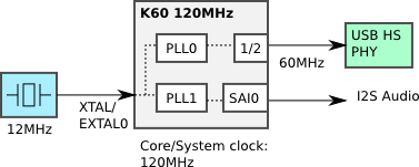
Figure 1 shows a summary of device clocking. I want to make both audio and system/USB clock from one 12MHz crystal.
Figure 1: Summary system clocking diagram
Question 1: Does the PLL can make 120MHz output from 12MHz crystal?
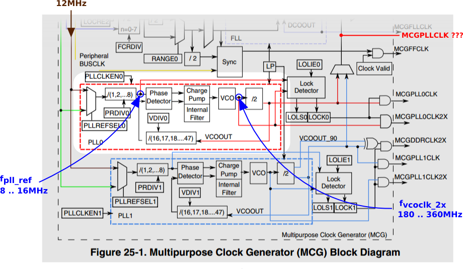
Figure 2 is a MCG block diagram extracted from reference manual.
The f_pll_ref and f_vcoclk_2x symbols are described on 'Table 15. MCG specifications' from datasheet.
K60 datasheet says, the valid frequency range of each signals are;
f_pll_ref: 8 MHz - 16Mhz
f_vcoclk_2x: 180 MHz - 360MHz
Now, we can make 120MHz from 12MHz with PRDIV0 = 2, VDIV0=20 settings.
MCGPLL0CLK = 12MHz / 2 * 20 / 2 * 2 = 120MHz
f_pll_ref = 12MHz / 2 = 6MHz (!!!)
f_vcoclk_2x = 240MHz
As you can see, f_pll_ref does NOT meet the constranits described on datasheet.
Can I get 120MHz system clock from 12MHz crystal?
Figure2: MCG block diagram
Question 2: Does the PLL1 can be used as a independent audio clock source for I2S/SAI module?
I want to make audio clock with PLL1 which is independent of system clock.
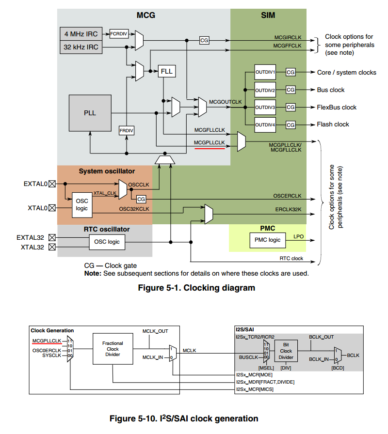
Figure 3 is a I2S/SAI clocking diagram of K60_100 series MCU. 'MCGPLLCLK' is connected to I2S/SAI module.
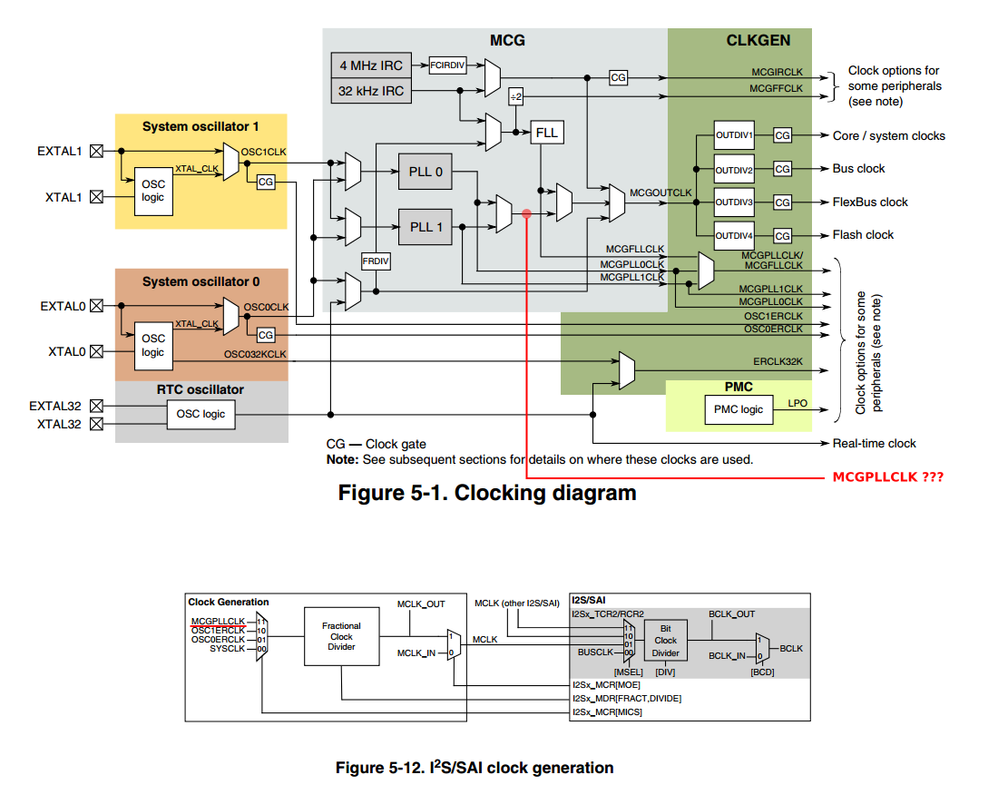
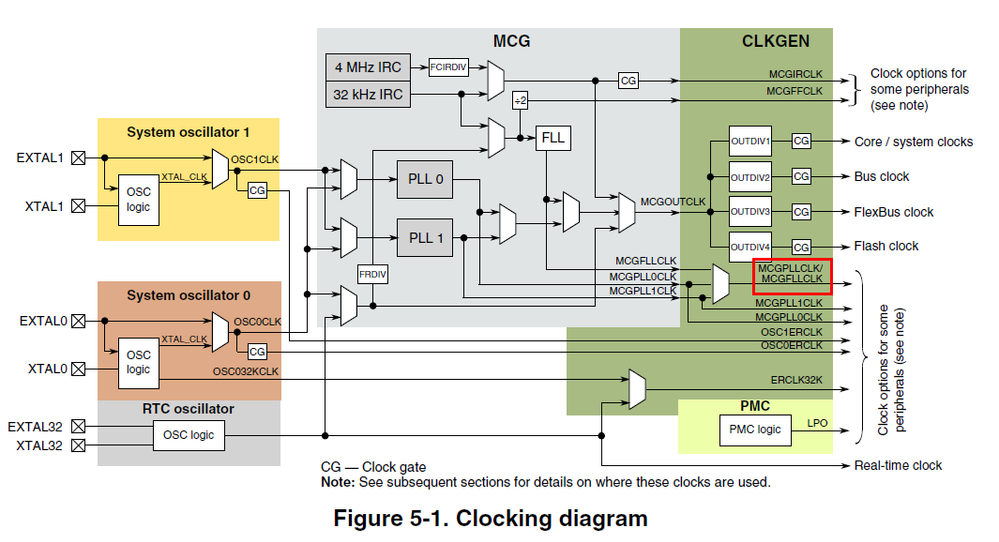
Figure 4 is K60_120 series MCU's one. Same 'MCGPLLCLK' is connected to I2S/SAI module, but it is not drawn in the MCG diagram.
I guess 'MCGPLLCLK' signal is a output of PLL0/1 selector. (But it means I can't get independent audio clock from PLL1..)
Figure 3: I2S/SAI clocking diagram of K60_100
Figure 4: I2S/SAI clocking diagram of K60_120/150
Regards,
Haruki Hasegawa
已解决! 转到解答。
Carlos,
Thank you for your information.
I noticed that I can use PLL0 for all clock sources.
I found a failure in my PLL calculation script. The acceptable error threshold was too small (< 0.001%) !
After fixed it, I found out many acceptable settings of PLL and fractional divider.
Regards,
Haruki Hasegawa
Hi,
1) THe PLL VCO output must be 2x than the requried CPU clock. This is, if you need a 120 CPU clock, the PLL VCO output must be 240Mhz.
Example :
Crystal = 50Mhz
PRDIV = 5
VDIV = 24
VCO_out = (50Mhz/5)*24
= 240Mhz
With this, we'll get:
MCGPLL0CLK2X = 240Mhz
MCGPLL0CLK = 120Mhz.
For your system we could use the following values:
Crystal = 12Mhz
PRDIV = 1
VDIV = 20
VCO_out = (12Mhz/1)*20
= 240Mhz
With this, we'll get:
MCGPLL0CLK2X = 240Mhz
MCGPLL0CLK = 120Mhz.
In both cases we keep the PLL reference in valid range, 10Mhz for the 50Mhz example and 12Mhz for your system.
2) MCGPLLCLK is the PLL selected for peripherals. On this device you can select FLL, PLL0 or PLL1 to be peripheral CLK. This is done on SIM_SOPT2 PLLFLLSEL[17:16].
This is shown on the Clock diagram. The FLL and PLLs outputs are connected to a MUX (selected by SIM_SOPT2[17:16]), the of this MUX is MCGPLLCLK/MCGFLLCLK:
This means that just one PLL can be used at a time to feed peripherals.
Why you're looking to use different PLL for the I2S?
Are you using a codec with built-in PLL?
Regards,
Carlos Neri
Hi, Carlos.
1) Is it true that the PLL diagram on reference manual is incorrect?
In the diagram on fig.25-1, the PLL feedback loop contains extra half divider, so it means PLL multiplication factor is (VDIV * 2).
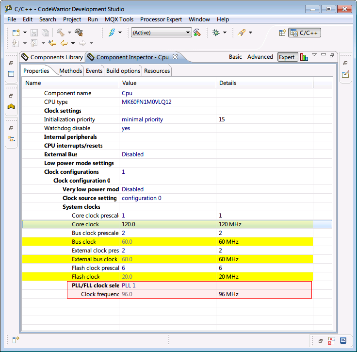
2) I tried to configure the settings which you said with Processor Expert.
PLL0: 120MHz (PRDIV0 = 1, VDIV0 = 20)
PLL1: 96MHz (PRDIV0 = 1, VDIV0 = 16)
SIM_SOPT2[17:16] PLLFLLSEL: PLL1
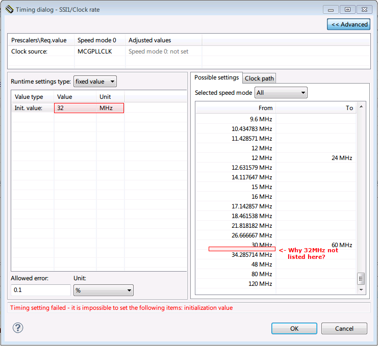
I2S0-MCLK: 32MHz = 96MHz / 3
(note: for ease of explanation, I choosed 32Mhz)
I tried to configure Processor Expert as described above, but it was impossible.
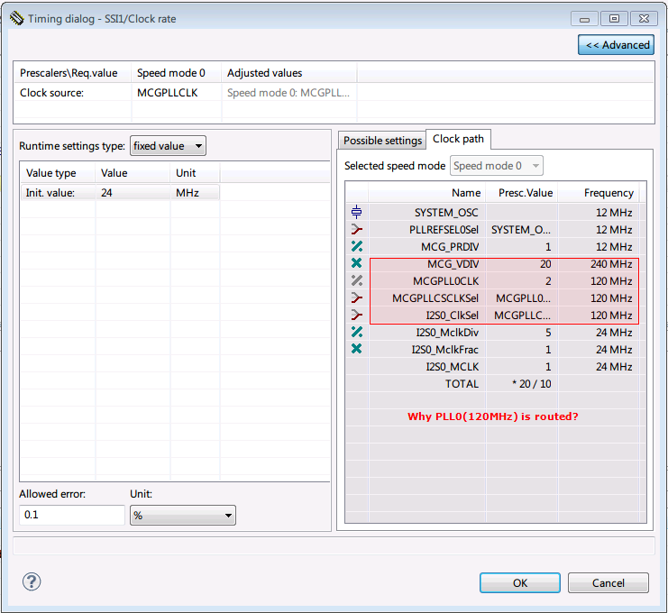
32 MHz was not listed on 'Possible settings'. PLL0 output was routed for I2S module though PLLFLLSEL bits was configured as PLL1.
Figure 5: PLL0: 120MHz, PLL1: 96MHz, PLLFLLSEL = PLL1
Figure 6: I2S0 MCLK settings (32MHz with a error)
Figure 7: I2S0 MCLK settings (24MHz, routed PLL0 clock?)
> Why you're looking to use different PLL for the I2S?
Several reasons;
- To achieve maximum performance, 120MHz is the best for system clock
- High-speed USB PHY reqires 60MHz (half of system clock)
- Reduce clock oscillators
- Audio clock cannot be maked from 120MHz system clock (e.g. 512*44.1kHz, 512*48kHz)
> Are you using a codec with built-in PLL?
No, the codec does not have a built-in PLL. K60 is the source of all I2S sygnals (MCLK, BCLK, LRCK, and DATA), and MCLK is connected through a jitter remover.
[K60] === (I2S) ==+-- (MCLK) -- [jitter remover] ---+===> [Codec]
\ /
+===== (BCLK, LRCK, DATA) ====+
Regards,
Haruki Hasegawa
Haruki,
I'll check with the documentation team on the feedback loop. I catch your point, the feedback is taken from the line already dvided by to and then sent it to the VDIV for the phase detector, adding an extra 2 to the divider.
On the PLL selection, you can get all the different CLK frequencies from the same 120Mhz PLL output:
- USB: You can use the integer and fractional dividers to get the 60Mhz for the HS. These are available on SIM_CLKDIV2, bits USBHSFRAC and USBHSDIV:
USB_CLK = DIV_Input*[(USBHSFRAC+1)/(USBHSDIV+1)]
The DIV_Input is selected on SIM_SOPT2, bits USBHSRC. If you configure PLL0 to 120Mhz and select PLL0 as the USB HS clock:
USBHSFRAC = 0
USBHSDIV = 1
USB_CLK = 120Mhz*((0+1)/(1+1))
USB_CLK = 60Mhz
For the MCLK is a similar situation, I2Sx_MCR bits MICS select the SAI MCLK input (use mux table you sent earlier) and I2Sx_MDR contains a fractional divider that can be used to calculate 512*44.1 or 512*48. The following formula is used:
MCLK = SAI_CLK_Input* ((FRACT+1)/(DIV+1))
For instance, 48*512 = 24.576Mhz and 120Mhz:
MCLK = 120Mhz*((127+1)/(624+1))
MCLK = 24.576Mhz
For 44.1*512 = 22.579200Mhz and 120Mhz, there is not an exact output, at least that I could find:
MCLK = 120Mhz*((88+1)/(472+1))
MCLK = 22.579281Mhz
With a 96Mhz CPU CLK a 44.1*512 can be achieved.
With all these, PLL1 won't be necessary since all CLK needed are derived from PLL0.
Regards,
Carlos Neri
Carlos,
Thank you for your information.
I noticed that I can use PLL0 for all clock sources.
I found a failure in my PLL calculation script. The acceptable error threshold was too small (< 0.001%) !
After fixed it, I found out many acceptable settings of PLL and fractional divider.
Regards,
Haruki Hasegawa
