- Forums
- Product Forums
- General Purpose MicrocontrollersGeneral Purpose Microcontrollers
- i.MX Forumsi.MX Forums
- QorIQ Processing PlatformsQorIQ Processing Platforms
- Identification and SecurityIdentification and Security
- Power ManagementPower Management
- Wireless ConnectivityWireless Connectivity
- RFID / NFCRFID / NFC
- Advanced AnalogAdvanced Analog
- MCX Microcontrollers
- S32G
- S32K
- S32V
- MPC5xxx
- Other NXP Products
- S12 / MagniV Microcontrollers
- Powertrain and Electrification Analog Drivers
- Sensors
- Vybrid Processors
- Digital Signal Controllers
- 8-bit Microcontrollers
- ColdFire/68K Microcontrollers and Processors
- PowerQUICC Processors
- OSBDM and TBDML
- S32M
- S32Z/E
-
- Solution Forums
- Software Forums
- MCUXpresso Software and ToolsMCUXpresso Software and Tools
- CodeWarriorCodeWarrior
- MQX Software SolutionsMQX Software Solutions
- Model-Based Design Toolbox (MBDT)Model-Based Design Toolbox (MBDT)
- FreeMASTER
- eIQ Machine Learning Software
- Embedded Software and Tools Clinic
- S32 SDK
- S32 Design Studio
- GUI Guider
- Zephyr Project
- Voice Technology
- Application Software Packs
- Secure Provisioning SDK (SPSDK)
- Processor Expert Software
- Generative AI & LLMs
-
- Topics
- Mobile Robotics - Drones and RoversMobile Robotics - Drones and Rovers
- NXP Training ContentNXP Training Content
- University ProgramsUniversity Programs
- Rapid IoT
- NXP Designs
- SafeAssure-Community
- OSS Security & Maintenance
- Using Our Community
-
- Cloud Lab Forums
-
- Knowledge Bases
- ARM Microcontrollers
- i.MX Processors
- Identification and Security
- Model-Based Design Toolbox (MBDT)
- QorIQ Processing Platforms
- S32 Automotive Processing Platform
- Wireless Connectivity
- CodeWarrior
- MCUXpresso Suite of Software and Tools
- MQX Software Solutions
- RFID / NFC
- Advanced Analog
-
- NXP Tech Blogs
- Home
- :
- General Purpose Microcontrollers
- :
- Kinetis Microcontrollers
- :
- Conditionally setup FTM Output Compare
Conditionally setup FTM Output Compare
- Subscribe to RSS Feed
- Mark Topic as New
- Mark Topic as Read
- Float this Topic for Current User
- Bookmark
- Subscribe
- Mute
- Printer Friendly Page
Conditionally setup FTM Output Compare
- Mark as New
- Bookmark
- Subscribe
- Mute
- Subscribe to RSS Feed
- Permalink
- Report Inappropriate Content
I am trying to use Output Compare to set (and clear) an FTM channel as a square-wave output, synchronized to a direct digital synthesis (DDS) waveform being generated by the same FTM module.
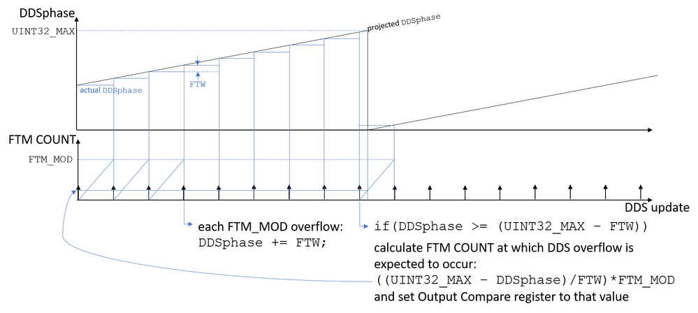
The FTM_MOD determines the update frequency of the 32-bit DDS phase accumulator. On each FTM overflow, the DDSphase accumulator is incremented by the frequency tuning word (FTW). When the phase accumulator is within a single FTW of overflowing, I calculate the FTM Count at which the projected DDS phase is expected to overflow, and set the Output Compare register to this value. (I am using the FTM_SetupOutputCompare() function from the fsl_ftm.c driver module to do so).
Strangely, when I observe the relative timing of the DDS update and the Output Compare "set", they are always separated by some fixed delay, and not by the value I have calculated. This fixed delay occurs regardless of the FTW (i.e. the DDS output frequency). The fixed delay also occurs if I manually set the Output Compare value to some fixed number less than FTM_MOD, instead of using the formula from the above figure. (For concreteness, the measured delay is almost one full FTM_MOD period).
Is there some reason that the Output Compare register would not be updated immediately?
- Mark as New
- Bookmark
- Subscribe
- Mute
- Subscribe to RSS Feed
- Permalink
- Report Inappropriate Content
The issue you describe when the software sync trigger time happens very close to FTM0 counter overflow makes sense... the GPIO is toggled late in the FTM period, so before the output compare is setup, the FTM begins a new cycle. Therefore, the SetOnMatch occurs two FTM cycles after the GPIO toggle, but really only one FTM cycle after the output compare is setup. If you put another GPIO toggle after the FTM_SetupOutputCompare(), you could verify this.
Can you explain why it is necessary to write a CnV value greater than MOD on cycles where there is no change in the FTM output compare? It really doesn't make sense to me what this command is doing, since the Output Compare operation should never be triggered (since CnV > MOD). Nevertheless, by adding that extra command (FTM_SetupOutputCompare() with CnV > MOD) into my project code, the Output Compare is now working reliably, and no longer exhibits the Output Compare toggle in the same period as the SetupOutputCompare call!
Also, can you explain which registers are relevant for Legacy PWM and which registers are relevant for Enhanced PWM Synchronization? The data sheet does a horrible job explaining the difference.
- Mark as New
- Bookmark
- Subscribe
- Mute
- Subscribe to RSS Feed
- Permalink
- Report Inappropriate Content
Hi Rudy,
I don't find the internal logic relationship about set CnV > MOD at reference manual.
What's the CnV>MOD setting will avoid to set the FTM0_CnSC [CHF] bit during non-operation output compare cycle.
I need to check with FTM module IP owner about observed behavior and related relationship.
About the legacy PWM synchronization and enhanced PWM synchronization selection via the register FTM0_SYNCONF[SYNCMODE] bit value.
Have a great day,
Mike
-----------------------------------------------------------------------------------------------------------------------
Note: If this post answers your question, please click the Correct Answer button. Thank you!
-----------------------------------------------------------------------------------------------------------------------
- Mark as New
- Bookmark
- Subscribe
- Mute
- Subscribe to RSS Feed
- Permalink
- Report Inappropriate Content
Thanks for the instructive example. I've set it up for my TWR-K64 board, to test the outputs and timing. Below is what I found, along with some proposed solutions.
Initial test
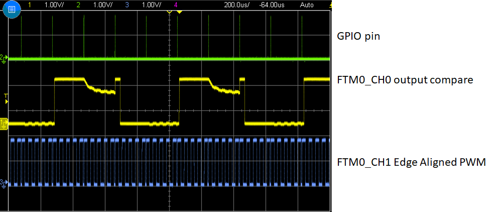
Running your code exactly as you attached it produces the above results. How did you generate your figures? Are those measured signals on an oscilloscope, or is it a simulated output? Anyway, there are two major problems with this code:
- Setting up the Output Compare with kFTM_NoOutputSignal causes the signal to decay.
- The FTM_SetSoftwareTrigger() call restarts the FTM counter at 0, so the CH1 period is not consistent if a trigger event occurs during the a given FTM cycle. This is because the FTM module is initialized with SWRSTCNT = 1.
First fix: don't use kFTM_NoOutputSignal
Instead of using kFTM_NoOutputSignal, I simply set up the Output Compare with whatever state the output is currently in. For example, if the output is in the high state, I call:
FTM_SetupOutputCompare(BOARD_FTM_BASEADDR, BOARD_FTM_OUT_CHANNEL, kFTM_SetOnMatch, compareValue);
And similarly if the output is in the low state, I use kFTM_ClearOnMatch. Since the compareValue is greater than MOD, these commands don't actually cause "set" or "clear" operations, but they do seem to prevent the signal droop shown in the first figure.
I'll note that I also found that this extra call to FTM_SetupOutputCompare(), in which a compareValue > MOD is used, is unnecessary. It simply changes the total delay between rising and falling edges out the Output Compare channel (since it involves a couple extra instructions).
Second fix: SWRSTCNT = 0
The documentation for the SWRSTCNT bit isn't very clear, but according to AN5142 (Features of the FlexTimer Module): "If the SWRSTCNT bit is set, the FTM counter restarts with FTM_CNTIN register value and the FTM_MOD and FTM_CnV registers are updated immediately. If the SWRSTCNT bit is cleared, the FTM counter continues to count normally and the FTM_MOD and FTM_CnV register update at the next loading point."
This suggests that the initial state of SWRSTCNT = 1 is the issue. As you can see from the first two figures, any time a GPIO toggle occurs, the FTM counter is restarted, and the PWM period is irregular.
Setting SWRSTCNT = 0 does fix the periodicity of the FTM0_CH1 PWM output (above). However, it also causes the Output Compare setup to never occur, and so the FTM0_CH0 output remains stuck in a low state.
Third fix: set up loading points at CNTMIN and CNTMAX
By default, the FTM is initialized with FTM_SYNC = 0b1000, (or SYNCHOM = 1, REINIT = 0, CNTMAX = 0, and CNTMIN = 0). With SWRSTCNT = 0, the FTM_SetSoftwareTrigger() no longer caused an immediate update of the CnV register, so I had to enable loading points. After setting CNTMIN = 1 and CNTMAX = 1, I found the following behavior:
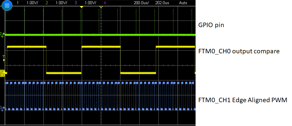
As you can see, the FTM0_CH0 output compare toggle always happens one FTM cycle after the output compare is set up. This is the desired and expected behavior with SWRSTCNT = 0, along with CNTMIN = 1 and CNTMAX = 1. So this all looks great.
But the issue remains for my DDS project:
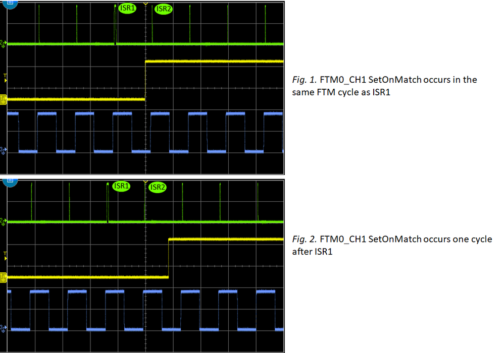
However, I tried to use the same FTM initialization for my DDS code in another project, and I no longer see the desired/expected behavior. As shown below, the SetOnMatch behavior is inconsistent. Sometimes, as in Fig. 1 the SetOnMatch occurs in the same period as FTM_SetupOutputCompare(). And other times, as in Fig. 2, the SetOnMatch occurs in the next FTM cycle (after ISR2).
I don't understand this non-deterministic behavior. As best I can tell, I have the FTM initialized the same way for both projects. That is:
FTM_MODE = 5 (0b101)
FTM_SYNC = 11 (0b1011)
FTM_COMBINE = 538976288 (0b100000001000000010000000100000)
FTM_SYNCONF = 7860 (0b1111010110100)
So again, I'm at an impasse as to why my code is behaving incorrectly.
- Mark as New
- Bookmark
- Subscribe
- Mute
- Subscribe to RSS Feed
- Permalink
- Report Inappropriate Content
Hi Andy,
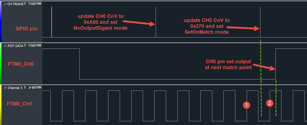
For I was using delay() function to update FTM0 CnV value, there should exist below issue for the software sync trigger time was very close to FTM0 counter overflow. So the output compare set will not set at the next cycle, would be delay to next next cycle. Please check attached signal for the detailed info.
If customer set the software sync trigger point not close to FTM counter overflow, this issue doesn't happen.
When I mask the below code and found below strange signal, which only happen once with whole captured signals scanning:
BOARD_FTM_BASEADDR->CONTROLS[BOARD_FTM_OUT_CHANNEL].CnV = 0xA00;
While, If I didn't mask above code, this strange signal never happened from captured siganls.
Thank you for the attention.
best regards,
Mike
- Mark as New
- Bookmark
- Subscribe
- Mute
- Subscribe to RSS Feed
- Permalink
- Report Inappropriate Content
Hi Andy,
Today, I did the test again.
About the output signal decay behavior, sorry for I am using software logic analyzer tool, I don't find that problem.
As your mentioned fix way, After change the FTM_SetupOutputCompare() function with previous compareMode, the issue was fixed.
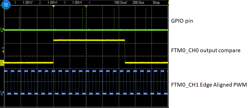
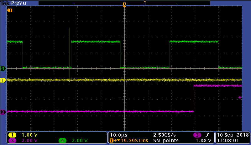
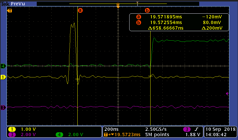
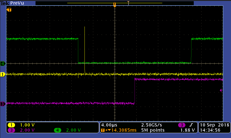
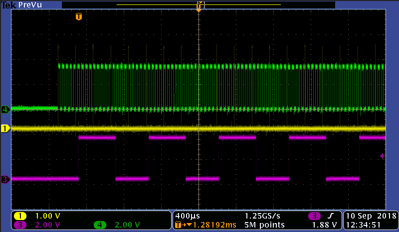
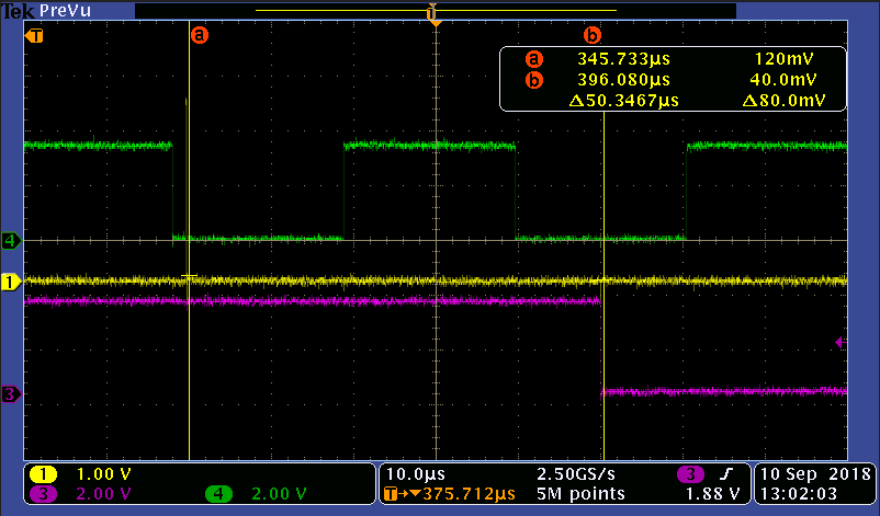
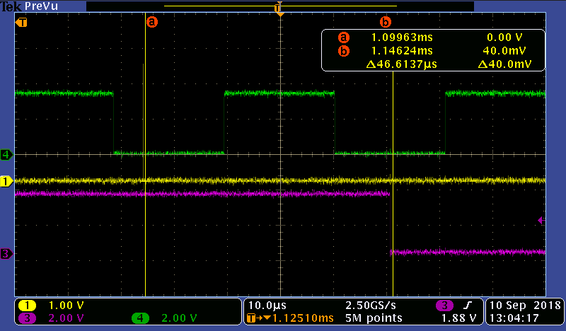
Today, I am using scope to measure the signals, the Yellow signal is GPIO toggle, Purple signal is output compare signal, the Green signal is edge aligned PWM. Below is overview scope screen picture:
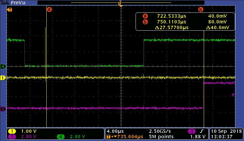
Below is the first output compare set (GPIO toggle to output set delta time is about 31us):
Below is the second output compare set (delta time is 27us).
You could find there with difference at different times software sync trigger with different delta time.
FTM0 counter is not clear during software sync trigger.
Below is the first output compare clear(delta time is 50us):
Below is the second output compare clear (delta time is 46us), which also shows the FTM0 counter is not clear by software sync trigger.
Then I checked the FTM0_SYNCONF[SWRSTCNT] bit, which is not set as expected.
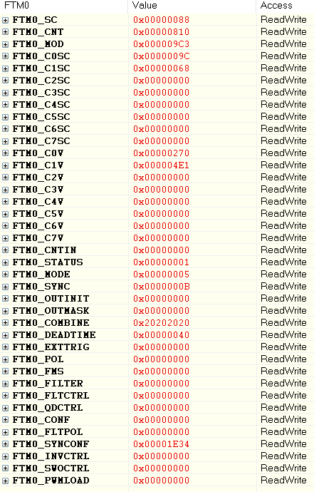
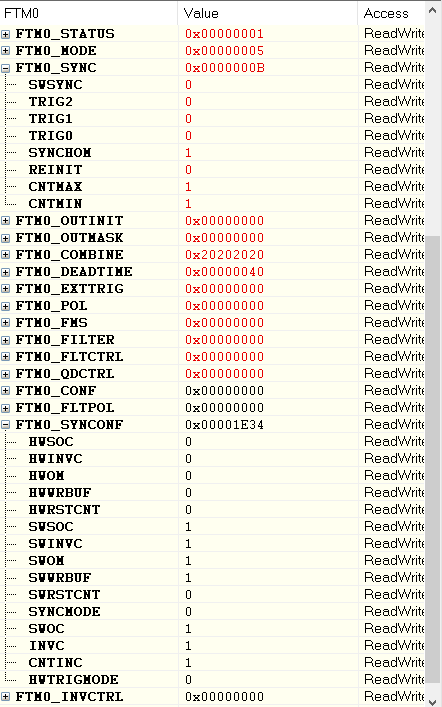
Please check my application FTM0 whole registers value:
From the registers value, it using the Legacy PWM synchronization mode.
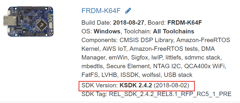
Please check your MCUXpresso SDK software for FRDM-K64F board version, I am using V2.4.2
I couldn't regenerate your mentioned second issue and third issue.
Thank you for the attention.
best regards,
Mike
- Mark as New
- Bookmark
- Subscribe
- Mute
- Subscribe to RSS Feed
- Permalink
- Report Inappropriate Content
It makes sense that you did not experience the same issues as I did, because you have initialized SWRSTCNT = 0 and FTM_SYNC = 0xB (which means CNTMAX = 1 and CNTMIN = 1). Therefore, your SetSoftwareTrigger does not cause the FTM counter to restart (since SWRSTCNT = 0), and you do have the max and min loading points enabled.
Therefore, your test code (based on ftm_output_compare.c) is behaving identically to mine. (See the screenshot from the section labeled "Third fix" above).
I will need to dig deeper to figure out why my actual project does not replicate this behavior.
- Mark as New
- Bookmark
- Subscribe
- Mute
- Subscribe to RSS Feed
- Permalink
- Report Inappropriate Content
Hi Andy,
I am using USB Logic analyzer tool to capture the output signals.
I will continue check your comments next week.
Thank you for the patience.
best regards,
Mike
- Mark as New
- Bookmark
- Subscribe
- Mute
- Subscribe to RSS Feed
- Permalink
- Report Inappropriate Content
I think I've found (in principle) a better way to do this, but I am unable to get it to work in practice. I would like to use the "intermediate load" function provided by the PWMLOAD register. The goal is to:
- calculate the Output Compare value, as described above
- write that value to the C(n)V register buffer
- on the next wrap around from MOD to CNTIN, load the C(n)V register with the buffered value
To implement this, I use the following code:
// 0. enable LDOK to enable loading of C(n)V register with its buffered value
FTM_0_PERIPHERAL->PWMLOAD |= (1U << 9);
// 1. calculate the Output Compare value
uint32_t compareValue;
compareValue = (uint32_t)(((float)(UINT32_MAX - DDS.phase)/FTW)*(COUNT_MOD+1)) & COUNT_MOD;
// 2. write the compare value to the C(n)V register buffer and setup the channel for "Set on Match"
uint32_t reg;
reg = FTM_0_PERIPHERAL->CONTROLS[1].CnSC; // capture the current state of the FTM register
reg &= ~(0x3C); // clear the MSnB:MSnA and ELSnB:ELSnA bits
reg |= 0x1C; // setup CnSC for "Set On Match"
FTM_0_PERIPHERAL->CONTROLS[1].CnSC = reg;
FTM_0_PERIPHERAL->CONTROLS[1].CnV = compareValue; // write the compareValue to the CnV buffer
If SYNCEN = 1 for CH1 (which is the channel I am using here), then the CH1 set always occurs almost one full FTM_MOD period after the compareValue is written to the CnV buffer, regardless of the value of compareValue.
If SYNCEN = 0 for CH1, then it appears that the compareValue is immediately written to the C(n)V register, and not to the buffer using the intermediate load.
What is the proper setup to FTM module to achieve the goal described above?
- Mark as New
- Bookmark
- Subscribe
- Mute
- Subscribe to RSS Feed
- Permalink
- Report Inappropriate Content
Hi,
From the above description, there need to make the FTM works in Output Compare mode.
The SDK provided FTM driver has below code to make the FTM works in Output compare mode:
It will clear all the [DECAPEN] & [COMBINE] & [CPWMS] bits setting.
Customer can enable the FTM timer to start output compare mode.
When customer want to change CnV value, customer can call the software sync trigger with SDK provided API function FTM_SetSoftwareTrigger().
I am using below code test FTM output compare CnV register modification.
BOARD_FTM_BASEADDR->MOD = 0x2000;
BOARD_FTM_BASEADDR->CONTROLS[BOARD_FTM_OUT_CHANNEL].CnV = 0x1000;
/* Update the buffered registers */
FTM_SetSoftwareTrigger(BOARD_FTM_BASEADDR, true);
FTM_StartTimer(BOARD_FTM_BASEADDR, kFTM_SystemClock);
.............
Delay one second here
............
BOARD_FTM_BASEADDR->MOD = 0x1000;
BOARD_FTM_BASEADDR->CONTROLS[BOARD_FTM_OUT_CHANNEL].CnV = 0x800;
/* Update the buffered registers */
FTM_SetSoftwareTrigger(BOARD_FTM_BASEADDR, true);
Wish it helps.
Have a great day,
Mike
-----------------------------------------------------------------------------------------------------------------------
Note: If this post answers your question, please click the Correct Answer button. Thank you!
-----------------------------------------------------------------------------------------------------------------------
- Mark as New
- Bookmark
- Subscribe
- Mute
- Subscribe to RSS Feed
- Permalink
- Report Inappropriate Content
Hi Mike,
Thanks for your patient explanations.
How do you have your FTM SYNCONF set up? I would like to use SWRSTCNT = 0, so that the CnV register is updated at the next loading point (i.e. on overflow) after FTM_SetSoftwareTrigger(BOARD_FTM_BASEADDR, true) is called, and not immediately when the software trigger is set.
Therefore, I am executing the following code:
// set SYNCONF so that the software trigger does not activate the FTM counter synchronization.
FTM_0_PERIPHERAL->SYNCONF &= ~(1U << 8);
// in the FTM overflow ISR:
// 1. calculate the Output Compare value
uint32_t compareValue;
compareValue = (uint32_t)(((float)(UINT32_MAX - DDS.phase)/FTW)*(COUNT_MOD+1)) & COUNT_MOD;
// 2. write the compare value to the C(n)V register buffer and setup the channel for "Set on Match"
FTM_SetupOutputCompare(FTM_0_PERIPHERAL, kFTM_Chnl_1, kFTM_SetOnMatch, compareValue);
FTM_SetSoftwareTrigger(FTM_0_PERIPHERAL, true); // enable loading of CnV register at next wraparound
However, this again results in a fixed delay between FTM_SetSoftwareTrigger and the actual SetOnMatch of the FTM0_CH1 output, regardless of the compareValue used for the Output Compare.
For your reference, the FTM SYNCONF register is set to: 0x00001eb4
And the FTM COMBINE register is set to: 0x20202020
- Mark as New
- Bookmark
- Subscribe
- Mute
- Subscribe to RSS Feed
- Permalink
- Report Inappropriate Content
Hi Andy,
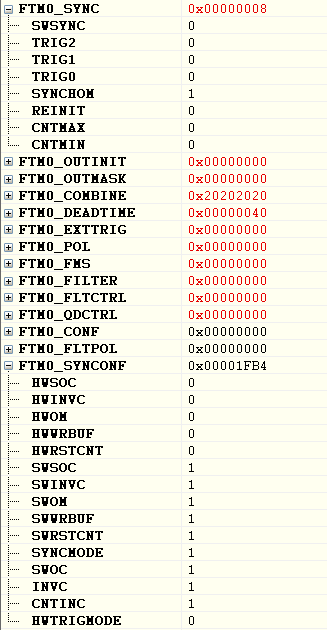
Please check below the FTM0_SYNC and FTM0_SYNCONF register value:
The FTM0_COMBINE register value is same with yours.
I tried another setting to use legacy PWM synchronization mode, while get the same result.
Below is the registers value:
Thank you for the attention.
Have a great day,
Mike
-----------------------------------------------------------------------------------------------------------------------
Note: If this post answers your question, please click the Correct Answer button. Thank you!
-----------------------------------------------------------------------------------------------------------------------
- Mark as New
- Bookmark
- Subscribe
- Mute
- Subscribe to RSS Feed
- Permalink
- Report Inappropriate Content
I do not get the same behavior for the two cases you've shown above (FTM0_SYNCONF = 0x00001FB4 and FTM0_SYNCONF = 0x00001E34).
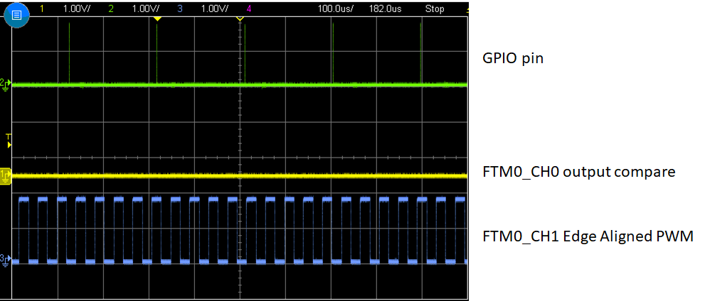
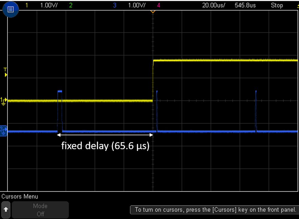
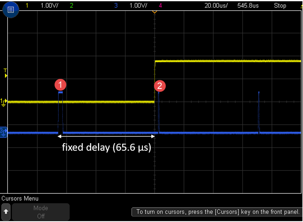
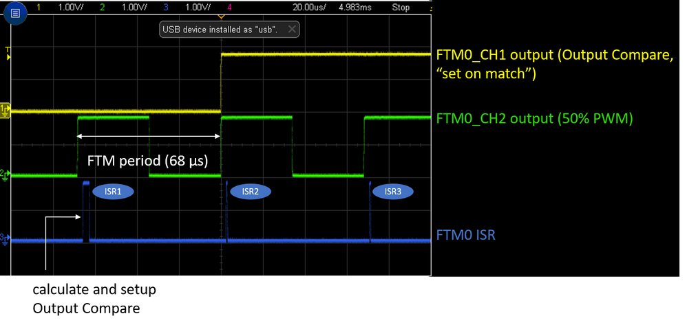
For FTM0_SYNCONF = 0x00001E34, with SWRSTCNT = 0 and SYNCMODE = 0, I measure the same fixed delay between the start of the FTM ISR and the FTM0_CH1 output set. My FTM_MOD = 4095, such that it is running at 14.648 kHz (a 68.3 µs period). I always measure 65.6 µs between the start of the overflow ISR and the output set (see picture below)
If instead, FTM0_SYNCONF = 0x00001FB4 (SWRSTCNT = 1 and SYNCMODE = 1), I get a variable delay between the start of the FTM ISR and the output compare set (which is the desirable behavior, as I'm using a new calculated value for Output Compare each time).
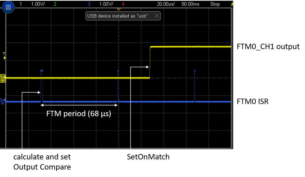
However, with this setting (SWRSTCNT = 1), the FTM_SetSoftwareTrigger call immediately writes the C(n)V register, and so the CH1 output is set in the same period as the output compare value is calculated. This is not desired. I would like to write the Output Compare value to the C(n)V buffer, and then have that buffered value loaded into the register at the next FTM overflow. As I understand it, this should be the behavior when SWRSTCNT = 0. However, when I clear that register bit, I get the fixed delay behavior shown in the top picture. Instead, I would like to achieve something like this:
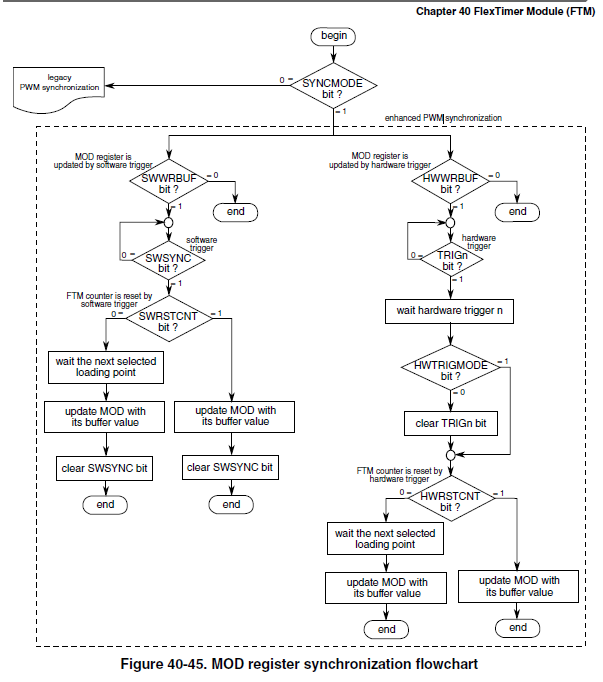
From the K64 Reference Manual, it seems that this type of behavior should be achievable either with SWRSTCNT = 0 (see below flow chart).
Does this flow chart also apply to C(n)V register synchronization? If so, then why, when I have SYNCMODE = 1, SWWRBUF = 1, and SWRSTCNT = 0, is the delay between the FTM ISR (which indicates FTM_CNT = 0) and the Output Compare Set a fixed value (discarding the calculated value for Output Compare)?
Alternatively, it seems that using the PWMLOAD register should also provide the functionality I am looking for, but I have also been unable to make that work (see my reply from August 23).
- Mark as New
- Bookmark
- Subscribe
- Mute
- Subscribe to RSS Feed
- Permalink
- Report Inappropriate Content
Hi Andy,
Sorry for the later reply.
From you latest post, the FTM interrupt happen with fixed frequency (14.648 kHz) is expected (MOD value is fixed).
While, I still have question about your application.
In below picture, you set FTM works in Output compare mode with match set at Interrupt service routine (ISR1). Right?
So, the CnV value also be set at ISR1.
What's the original CnV value before enter into ISR1? (If original CnV value more then MOD?)
If you using the FTM0_SYNCONF = 0x00001FB4 (SWRSTCNT = 1 and SYNCMODE = 1) with software sync trigger.
The FTM_SetSoftwareTrigger call immediately writes the C(n)V register is expected.
Base on above behavior, If you could set FTM module working mode (output compare mode) at ISR2?
If yes, then you could set the CnV value with required counter number and software trigger SYNC to write CnV register value with (FTM0_SYNCONF = 0x00001FB4 (SWRSTCNT = 1 and SYNCMODE = 1)).
Thank you for the attention.
Have a great day,
Mike
-----------------------------------------------------------------------------------------------------------------------
Note: If this post answers your question, please click the Correct Answer button. Thank you!
-----------------------------------------------------------------------------------------------------------------------
- Mark as New
- Bookmark
- Subscribe
- Mute
- Subscribe to RSS Feed
- Permalink
- Report Inappropriate Content
Yes, the FTM interrupt frequency is expected to be 14.648 kHz (MOD value is fixed at 4095).
In ISR1, I am:
- calculating the output compare value, compareValue
- setting up Output Compare by calling FTM_SetupOutputCompare(FTM_0_PERIPHERAL, kFTM_Chnl_1, kFTM_SetOnMatch, compareValue)
- setting the software trigger by calling FTM_SetSoftwareTrigger(FTM_0_PERIPHERAL, true)
As you point out, if FTM0_SYNCONF = 0x00001FB4 (SWRSTCNT = 1 and SYNCMODE = 1), then the above sequence immediately writes the C(n)V register, and the Output Compare also occurs in ISR1. This is almost what I need except that sometimes, by the time step 3 has executed, the output compare value that I calculate is less than the current FTM_CNT value. Therefore, my idea is to always calculate the output compare value in ISR1, but wait to execute the SetOnMatch until the next FTM cycle. On that next FTM cycle, if the C(n)V value is loaded at FTM_CNT = 0, then the SetOnMatch can occur anywhere in the FTM cycle (from FTM_CNT = 0 to 4095), since I don't have to wait for the 3 steps of ISR execution listed above. This is why I would like to use the SWRSTCNT = 0 bit to wait until the next loading point to write the C(n)V register with its buffered value.
To answer your other question regarding the previous C(n)V value: briefly put, the C(n)V value I calculate is always less than MOD.
A longer explanation: as I mentioned in the original post, I am trying to use the Output Compare to generate a square wave with 50% duty cycle, whose edges are synchronized to a DDS waveform of arbitrary frequency. Each time the DDS 32-bit phase accumulator wraps from UINT32_MAX to 0, I generate a rising edge. And when the phase accumulator passes from UINT32_MAX/2 to (UINT32_MAX/2+1), I generate a falling edge. (This is the goal anyway). Therefore, when the rising edge Output Compare C(n)V is calculated for a SetOnMatch event (as in the above scope traces), the previous C(n)V value was used for a ClearOnMatch event (falling edge). The C(n)V value is variable for each DDS cycle (since the DDS period is variable, and has no fixed relationship to the FTM frequency of 14.648 kHz), but again, C(n)V is always be less than MOD. In fact the formula I use for the rising and falling edges guarantees it:
For rising edges:
compareValue = (uint32_t)(((float)(UINT32_MAX - DDS.phase)/FTW)*(COUNT_MOD+1)) & COUNT_MOD;
For falling edges:
compareValue = (uint32_t)(((float)(UINT32_HALFMAX - DDS.phase)/FTW)*(COUNT_MOD+1)) & COUNT_MOD;
where COUNT_MOD = 4095. Because of the final bitwise AND operation at the end of each formula, compareValue is strictly <= 4095.
Thanks for your continued help.
- Mark as New
- Bookmark
- Subscribe
- Mute
- Subscribe to RSS Feed
- Permalink
- Report Inappropriate Content
Hi,
Thank you for the detailed info.
I think the blue signal is generated by software to toggle a GPIO pin when the FTM timer overflow happened (in FTM interrupt).
Why yellow rising edge is before the second blue rising edge?
I think you set the CnV value is quite close to CNTIN value, the FTM counter doesn't stop counting when enter into interrupt service routine. So the output compare channel set before the GPIO toggle.
Have you tried the FTM PWM load function? What's the behavior of that function?
Have a great day,
Mike
-----------------------------------------------------------------------------------------------------------------------
Note: If this post answers your question, please click the Correct Answer button. Thank you!
-----------------------------------------------------------------------------------------------------------------------
- Mark as New
- Bookmark
- Subscribe
- Mute
- Subscribe to RSS Feed
- Permalink
- Report Inappropriate Content
The questions you have asked are exactly my questions. I don't understand why the yellow rising edge occurs before the second blue rising edge. As I understand it, when SWRSTCNT = 0, the C(n)V register value is loaded at the next loading point after SWSYNC is set. However, when I use SWRSTCNT = 0, calculate a variable compareValue, and then set SWSYNC, I get the fixed delay behavior shown (65.6 µs between the start of ISR1 and the yellow rising edge). This doesn't make sense to me. The C(n)V value will be different on each cycle, so generally takes on a random value between CNTIN and MOD, and yet the delay is always 65.6 µs.
I have tried using PWMLOAD instead of SWRSTCNT. Please see my reply from August 23. Unfortunately, it results in the same behavior as when I use SWRSTCNT = 0. That is, if SYNCEN = 1 for CH1 (which is the channel I am using here), then the CH1 set always occurs almost one full FTM_MOD period after the compareValue is written to the CnV buffer, regardless of the value of compareValue. And if SYNCEN = 0 for CH1, then the compareValue is immediately written to the C(n)V register, and not to the buffer using the intermediate load.
Because the blue channel in the scope traces is generated by a software toggle of a GPIO pin, I added another output pin to the FTM module and set it to output a 50% duty cycle PWM signal at the FTM frequency. This provides a hardware-defined reference for where the FTM wrap-around occurs. This makes obvious that the Output Compare (yellow) channel is set when FTM_CNT = CNTIN, even though the Output Compare value is not equal to CNTIN.
- Mark as New
- Bookmark
- Subscribe
- Mute
- Subscribe to RSS Feed
- Permalink
- Report Inappropriate Content
Hi Andy,
I did a test with FRDM-K64F board.
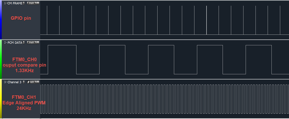
The FTM0 refer clock is 60MHz, using FTM0_CH1 pin generate 24KHz Edge-Aligned PWM signal(High-true pulses
(clear Output on match)) with 50% duty cycle as FTM counter monitor.
The FTM0 MOD value is fixed to 0x9C3 (60MHz/24KHz = 2500).
FTM0_CH0 pin as output compare pin will generate square signal with 1.33KHz .
I use a delay() function to emulate modify FTM0_CH0 output compare mode and CnV value periodically.
There is a GPIO pin will toggle after each delay() function to detect/verify the CnV value actual load point.
Below is the overall signals:
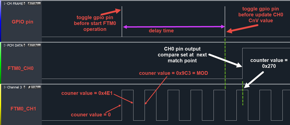
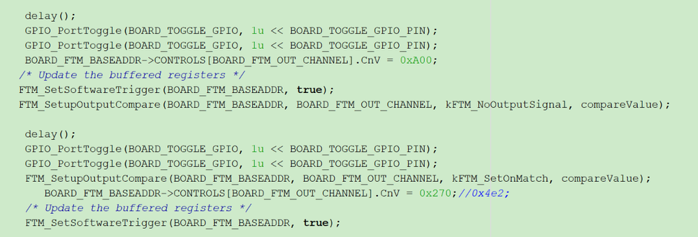
During FTM0 module initialization, I set the FTM0_CH0 pin output compare value to 0xA00 (more than MOD register value (0x9C3)) with below code:
uint32_t compareValue = 0xA00;
/* Setup the output compare mode to toggle output on a match */
FTM_SetupOutputCompare(BOARD_FTM_BASEADDR, BOARD_FTM_OUT_CHANNEL, kFTM_SetOnMatch, compareValue);
FTM_StartTimer(BOARD_FTM_BASEADDR, kFTM_SystemClock);
GPIO_PortToggle(BOARD_TOGGLE_GPIO, 1u << BOARD_TOGGLE_GPIO_PIN);
GPIO_PortToggle(BOARD_TOGGLE_GPIO, 1u << BOARD_TOGGLE_GPIO_PIN);
Then after delay to set FTM0_CH0 pin CnV value to 0x270 (half of the CH1 PWM high voltage) with below code:
delay();
GPIO_PortToggle(BOARD_TOGGLE_GPIO, 1u << BOARD_TOGGLE_GPIO_PIN);
GPIO_PortToggle(BOARD_TOGGLE_GPIO, 1u << BOARD_TOGGLE_GPIO_PIN);
BOARD_FTM_BASEADDR->CONTROLS[BOARD_FTM_OUT_CHANNEL].CnV = 0x270;
/* Update the buffered registers */
FTM_SetSoftwareTrigger(BOARD_FTM_BASEADDR, true);
Below is actual signal:
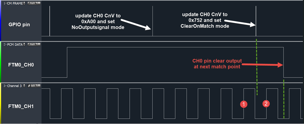
After the first CH0 output compare set match, before set CH0 pin clear on match.
It need to set the CH0 pin with no output signal setting and CnV change back to 0xA00 (more than MOD) with below code.
Then we can set CH0 with clear on match mode and update CnV value to 0x752 (middle of CH1 PWM low voltage):
Below is the actual signal:
With the similar code, before next CH0 set on match, it need to set the CH0 pin with no output signal setting and CnV change back to 0xA00 (more than MOD). The actual signal is below:
I think you could refer above code at your application FTM interrupt service routine.
My test project is based on MCUXpresso SDK for FRDM-K64F board [output_compare] project with default path:
..\FRDM-K64F\boards\frdmk64f\driver_examples\ftm\output_compare
Please check detailed info with attached source code.
Wish it helps.
Have a great day,
Mike
-----------------------------------------------------------------------------------------------------------------------
Note: If this post answers your question, please click the Correct Answer button. Thank you!
-----------------------------------------------------------------------------------------------------------------------
- Mark as New
- Bookmark
- Subscribe
- Mute
- Subscribe to RSS Feed
- Permalink
- Report Inappropriate Content
Hi Andy,
I am doing a test with FRDM-K64F board.
I will let you know my test result later.
Thank you for the patience.
Have a great day,
Mike
-----------------------------------------------------------------------------------------------------------------------
Note: If this post answers your question, please click the Correct Answer button. Thank you!
-----------------------------------------------------------------------------------------------------------------------
- Mark as New
- Bookmark
- Subscribe
- Mute
- Subscribe to RSS Feed
- Permalink
- Report Inappropriate Content
Hi,
The fixed delay was caused by MOD register update.
In general, the MOD register value isn't updated when the new value written into the register.
The MOD register synchronization will bring that delay.
Thank you for the attention.
Have a great day,
Mike
-----------------------------------------------------------------------------------------------------------------------
Note: If this post answers your question, please click the Correct Answer button. Thank you!
-----------------------------------------------------------------------------------------------------------------------
- Mark as New
- Bookmark
- Subscribe
- Mute
- Subscribe to RSS Feed
- Permalink
- Report Inappropriate Content
I am not updating the MOD register. I am updating only the CnV register. According to table 40.4.10.3 CnV Register update, if CLKS[1:0] ≠ 0:0, and FTMEN = 1 (which is the case here), the CnV register us updated:
- If the selected mode is output compare then CnV register is updated
according to the SYNCEN bit. If (SYNCEN = 0) then CnV register is updated
after CnV register was written at the next change of the FTM counter, the
end of the prescaler counting. If (SYNCEN = 1) then CnV register is updated
by the C(n)V and C(n+1)V register synchronization. - If the selected mode is not output compare and (SYNCEN = 1) then CnV
register is updated by the C(n)V and C(n+1)V register synchronization.
Here is the FTM configuration I am using:
const ftm_config_t FTM_0_config = {
.prescale = kFTM_Prescale_Divide_1,
.bdmMode = kFTM_BdmMode_0,
.pwmSyncMode = kFTM_SoftwareTrigger,
.reloadPoints = 0,
.faultMode = kFTM_Fault_Disable,
.faultFilterValue = 0,
.deadTimePrescale = kFTM_Deadtime_Prescale_1,
.deadTimeValue = 0,
.extTriggers = kFTM_InitTrigger,
.chnlInitState = 0,
.chnlPolarity = 0,
.useGlobalTimeBase = false
};
By checking the SYNCEN bit of the COMBINE register, I discovered that I'm actually in the second case described above, where the "CnV register is updated by the C(n)V and C(n+1)V register synchronization."
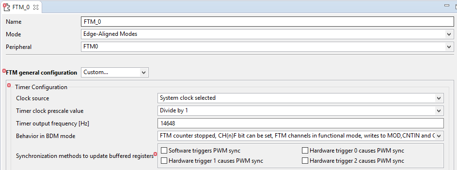
I am using MCUXpresso Config Tools to initialize this FTM module. Am I able disable SYNCEN from there? If I uncheck all "Synchronization methods," the configuration throws an error (see below).
I'm not actually using FTM_0 for PWM, but the only modes available to me are:
1. Edge-Aligned Modes
2. Center-Aligned PWM Mode
3. Quadrature Decoder Mode
Why is there no "Output Compare" mode selectable?
