- Forums
- Product Forums
- General Purpose MicrocontrollersGeneral Purpose Microcontrollers
- i.MX Forumsi.MX Forums
- QorIQ Processing PlatformsQorIQ Processing Platforms
- Identification and SecurityIdentification and Security
- Power ManagementPower Management
- Wireless ConnectivityWireless Connectivity
- RFID / NFCRFID / NFC
- Advanced AnalogAdvanced Analog
- MCX Microcontrollers
- S32G
- S32K
- S32V
- MPC5xxx
- Other NXP Products
- S12 / MagniV Microcontrollers
- Powertrain and Electrification Analog Drivers
- Sensors
- Vybrid Processors
- Digital Signal Controllers
- 8-bit Microcontrollers
- ColdFire/68K Microcontrollers and Processors
- PowerQUICC Processors
- OSBDM and TBDML
- S32M
- S32Z/E
-
- Solution Forums
- Software Forums
- MCUXpresso Software and ToolsMCUXpresso Software and Tools
- CodeWarriorCodeWarrior
- MQX Software SolutionsMQX Software Solutions
- Model-Based Design Toolbox (MBDT)Model-Based Design Toolbox (MBDT)
- FreeMASTER
- eIQ Machine Learning Software
- Embedded Software and Tools Clinic
- S32 SDK
- S32 Design Studio
- GUI Guider
- Zephyr Project
- Voice Technology
- Application Software Packs
- Secure Provisioning SDK (SPSDK)
- Processor Expert Software
- Generative AI & LLMs
-
- Topics
- Mobile Robotics - Drones and RoversMobile Robotics - Drones and Rovers
- NXP Training ContentNXP Training Content
- University ProgramsUniversity Programs
- Rapid IoT
- NXP Designs
- SafeAssure-Community
- OSS Security & Maintenance
- Using Our Community
-
- Cloud Lab Forums
-
- Knowledge Bases
- ARM Microcontrollers
- i.MX Processors
- Identification and Security
- Model-Based Design Toolbox (MBDT)
- QorIQ Processing Platforms
- S32 Automotive Processing Platform
- Wireless Connectivity
- CodeWarrior
- MCUXpresso Suite of Software and Tools
- MQX Software Solutions
- RFID / NFC
- Advanced Analog
-
- NXP Tech Blogs
- Home
- :
- CodeWarrior
- :
- CodeWarrior Development Tools
- :
- Can't read the UART Data register
Can't read the UART Data register
- Subscribe to RSS Feed
- Mark Topic as New
- Mark Topic as Read
- Float this Topic for Current User
- Bookmark
- Subscribe
- Mute
- Printer Friendly Page
- Mark as New
- Bookmark
- Subscribe
- Mute
- Subscribe to RSS Feed
- Permalink
- Report Inappropriate Content
Hi everyone,
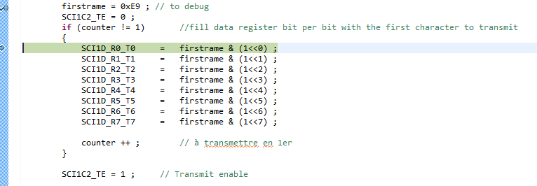
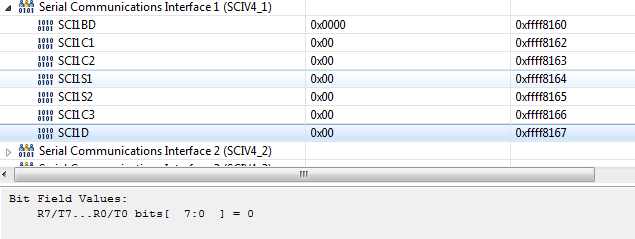
I work on codewarrior 10.6 with a multilink universal on a ship MCF51CN128. I created a program to make the UART work, so, in a transmit test, i realized it didn't work, so, i debugged it and realized i couldn't read the Data register and also that when i use the SCI1 , my configuration wasn't write on the registers. I made a little try on the SCI2, and when i filled the data register, i couldn't see it either, but, whe i finished to fill it, the "data full" flag worked successfully.
So i don't understand from where it could come from, the SCI transmit is not enable when we fill the data register.
Any ideas of where it could come from?
Thanks for your help !
Adrien Segura
Solved! Go to Solution.
- Mark as New
- Bookmark
- Subscribe
- Mute
- Subscribe to RSS Feed
- Permalink
- Report Inappropriate Content
Did you set bitrate properly? Are you sure you are using proper pins? Doesn't code from your last message stuck at some point? If it doesn't stuck then byte should be send. If Codewarrior Processor Expert supports MCF51CN try doing new project and initializing SCI1, check if it works, perhaps try SCI PE initialization code in your project.
It's from several microseconds to milliseconds SCI byte transfers and TC is 0. TDRE is 0 even shorter unless you buffer 2nd byte. You can't monitor these with debugger. More over for proper SCI operation you should remove SCI data and status register from watchpoints, as well make debugger memory window not including these registers. Read operations are part of SCI flags clear / data queue removal operation, only your code should read them, debugger should not touch them by any means. Shouldn't be a big problem for Tx function, perhaps it will function having SCI regs included in memory window, but really a problem for Rx.
- what they exactly mean by "read the SCixS1" ? read the entire register like we did earlier, or just reading one bit of the register is enough?
You can't read just a bit, you also can't write just a bit. It's impossible. Bits are not addressable, only bytes are. Every time you read bit using bit define CPU reads whole register. When you write just one bit you let CPU read whole byte, modify byte to make bit set or cleared, then write resulting byte back. Even dedicated bit set bit clear CPU instructions behave exactly the same, read whole byte, modify it, write whole byte back.
- Same for the time during steps : should i put the steps succesively with nothing between them or is it tolerate?
It doesn't matter how long is pause between read of S1 and write/read access to D, you may insert something in between.
- Mark as New
- Bookmark
- Subscribe
- Mute
- Subscribe to RSS Feed
- Permalink
- Report Inappropriate Content
Reads from and write to data register have different meanings. You write data to send and read data received, you can't verify what you wrote to data register! Debugger won't show what you wrote to data register.
As well your setting data register bit by bit doesn't make any sense. You need to write and read it simultaneously all bits at once. All writes and reads from data register should be coupled with proper corresponding status bits clear. To send data you need to read status register, and then write data register. To read received value you need as well read status register and then read data register. It won't work properly without leading read of status register.
So again, to send you need to read status register, then write to data register. This will initiate data transfer. What happens if you read status register, and then "set just one bit"? OK, 1) you read status bit, which initiates read/send sequence, SCI module doesn't yet know, are you going to send or read received data. Then 2) CPU reads data register, sets the bit "in memory" and finally 3) writes resulting byte pattern back to data register. As you may see byte send requirement is violated, you don't read status register again between steps 2 and 3. This is one of examples where bitfields like SCI1D_R0_T0 fail.
- Mark as New
- Bookmark
- Subscribe
- Mute
- Subscribe to RSS Feed
- Permalink
- Report Inappropriate Content
Hi,
Thanks for your answer, it helps a lot.
For the bit per bit assignment , i wasn't sure it was a problem, so i used the safest way.
You said that it was writing on the data register that initiate the transfer. I though it was the Transmit Enable Bit.
I already had made the read status register to clear the flags, but only after the transmission, i didnt know i had to do it
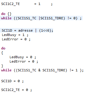
before. I tried what u said and, with the scope , i still don't have any data transmit. my code looks like this (simplified):
the first while is to read the status register before transmit as you said, then i fill the data transmit, so i should begin the transmission.
then , the second while is to wait the end of the transmission, reset the flags by writing something on the data register and stop the transmit mode.
Do you have any ideas of what could be my problem? thanks already for your help !
Adrien Segura
- Mark as New
- Bookmark
- Subscribe
- Mute
- Subscribe to RSS Feed
- Permalink
- Report Inappropriate Content
I forgot to tell !
even with your modifications, i still have a configuration problem : as u can see above, non of my registers are configured, wich is strange because i did configurate them. More strange : they all are at the value 0x00 , but, the reset value (for the register SCIBD for exemple) is different. The others SCI registers (SCI2-3) that i didn't touch doesn't have this problem.
Any ideas?
Thanks for your help !
Adrien Segura
- Mark as New
- Bookmark
- Subscribe
- Mute
- Subscribe to RSS Feed
- Permalink
- Report Inappropriate Content
Bitfields aren't the safest way. Period.
TE bit is normally set during initialization. No, it's not used to initiate transfer. Normal operation is
while( (SCI1S1 & SCI1S1_TDRE_MASK)==0 )
{}
, then write new data.
Please don't insert not editable code screenshots. Your first do loop is not right. 1) first of all TC bit is applicable only for something like half duplex RS485. You wait for TransferComplete, then turn off transmitter or something like that. Your 2nd loop waiting for TC is appropriate if you really want to disable SCI Tx after transfer. 2) But in first loop you keep looping while TDRE (or TC) is set. It is forever loop, TDRE won't clear without initiating new transfer. You should
while(TDRE==0){}.
Regarding SCI1 configuration problem, didn't you gate clocks to SCi1 module? You need to check SCGC1.
Regards,
Edward
- Mark as New
- Bookmark
- Subscribe
- Mute
- Subscribe to RSS Feed
- Permalink
- Report Inappropriate Content
Hi,
Thnaks for your answer, for the SCI1 configuration problem, you were right, don't know why but i disabled the SCI1 clock module.
I tried what you told me to do, but the TC and TDRE flags seems to not clear themselves even when following step by step the procedure : reading SCI1 module while they are set , then writing the data register.
SCI1C2_TE = 1 ;
while( (SCI1S1 & SCI1S1_TDRE_MASK & SCI1S1_TC_MASK)== 0 )
{}
SCI1D = 0xAA ;
do
{
LedBusy = 0 ;
LedError = 0 ;
}
while ((SCI1S1_TC & SCI1S1_TDRE) != 1 );
SCI1C2_TE = 0 ;
The TC and TDRE flag are initialized at 1, so they pass each while without any problem. But the should have been cleared when i wrote the data register. Maybe a problem of configuration? I just changed the baud rate divisor and the inversion data bits to transmit and receive.
By the way, my UART is to communicate on RS485, and when i looked to the signal, it seems that i have a transmission, but it's just a constant logic 1, my data was 0xAA , pretty simple to read.
Any ideas of what could be the problem?
- Mark as New
- Bookmark
- Subscribe
- Mute
- Subscribe to RSS Feed
- Permalink
- Report Inappropriate Content
while( (SCI1S1 & SCI1S1_TDRE_MASK & SCI1S1_TC_MASK)== 0 )
this is not correct again. First bitwise & in the best case gives SCI1S1_TDRE_MASK, second & gives 0. Why don't you wait there only for TDRE?
- Mark as New
- Bookmark
- Subscribe
- Mute
- Subscribe to RSS Feed
- Permalink
- Report Inappropriate Content
Hi,
I also tried this earlier, but i had the same result with that code :
SCI1C2_TE = 1 ;
while((SCI1S1 & SCI1S1_TDRE_MASK )== 0 )
{}
SCI1D = 0xAA ;
do
{
LedBusy = 0 ;
LedError = 0 ;
}
while ((SCI1S1_TC & SCI1S1_TDRE) != 1 );
SCI1C2_TE = 0 ;
Also, if i want to wait for the TC bit is because i use an RS485, so i have to clear that bit too. While in debugger, i saw that the flags didn't clear themselves even with your procedure.The reference manual says about those bits :
i didn't put everything, just the useful to clear the bits.For both, it should have worked. Do you know what they exactly mean by "read the SCixS1" ? read the entire register like we did earlier, or just reading one bit of the register is enough?
Same for the time during steps : should i put the steps succesively with nothing between them or is it tolerate?
Thanks for your help, you already helped me a lot !
Adrien Segura
- Mark as New
- Bookmark
- Subscribe
- Mute
- Subscribe to RSS Feed
- Permalink
- Report Inappropriate Content
Did you set bitrate properly? Are you sure you are using proper pins? Doesn't code from your last message stuck at some point? If it doesn't stuck then byte should be send. If Codewarrior Processor Expert supports MCF51CN try doing new project and initializing SCI1, check if it works, perhaps try SCI PE initialization code in your project.
It's from several microseconds to milliseconds SCI byte transfers and TC is 0. TDRE is 0 even shorter unless you buffer 2nd byte. You can't monitor these with debugger. More over for proper SCI operation you should remove SCI data and status register from watchpoints, as well make debugger memory window not including these registers. Read operations are part of SCI flags clear / data queue removal operation, only your code should read them, debugger should not touch them by any means. Shouldn't be a big problem for Tx function, perhaps it will function having SCI regs included in memory window, but really a problem for Rx.
- what they exactly mean by "read the SCixS1" ? read the entire register like we did earlier, or just reading one bit of the register is enough?
You can't read just a bit, you also can't write just a bit. It's impossible. Bits are not addressable, only bytes are. Every time you read bit using bit define CPU reads whole register. When you write just one bit you let CPU read whole byte, modify byte to make bit set or cleared, then write resulting byte back. Even dedicated bit set bit clear CPU instructions behave exactly the same, read whole byte, modify it, write whole byte back.
- Same for the time during steps : should i put the steps succesively with nothing between them or is it tolerate?
It doesn't matter how long is pause between read of S1 and write/read access to D, you may insert something in between.


