- Forums
- Product Forums
- General Purpose MicrocontrollersGeneral Purpose Microcontrollers
- i.MX Forumsi.MX Forums
- QorIQ Processing PlatformsQorIQ Processing Platforms
- Identification and SecurityIdentification and Security
- Power ManagementPower Management
- MCX Microcontrollers
- S32G
- S32K
- S32V
- MPC5xxx
- Other NXP Products
- Wireless Connectivity
- S12 / MagniV Microcontrollers
- Powertrain and Electrification Analog Drivers
- Sensors
- Vybrid Processors
- Digital Signal Controllers
- 8-bit Microcontrollers
- ColdFire/68K Microcontrollers and Processors
- PowerQUICC Processors
- OSBDM and TBDML
-
- Solution Forums
- Software Forums
- MCUXpresso Software and ToolsMCUXpresso Software and Tools
- CodeWarriorCodeWarrior
- MQX Software SolutionsMQX Software Solutions
- Model-Based Design Toolbox (MBDT)Model-Based Design Toolbox (MBDT)
- FreeMASTER
- eIQ Machine Learning Software
- Embedded Software and Tools Clinic
- S32 SDK
- S32 Design Studio
- GUI Guider
- Zephyr Project
- Voice Technology
- Application Software Packs
- Secure Provisioning SDK (SPSDK)
- Processor Expert Software
- MCUXpresso Training Hub
-
- Topics
- Mobile Robotics - Drones and RoversMobile Robotics - Drones and Rovers
- NXP Training ContentNXP Training Content
- University ProgramsUniversity Programs
- Rapid IoT
- NXP Designs
- SafeAssure-Community
- OSS Security & Maintenance
- Using Our Community
-
- Cloud Lab Forums
-
- Knowledge Bases
- ARM Microcontrollers
- i.MX Processors
- Identification and Security
- Model-Based Design Toolbox (MBDT)
- QorIQ Processing Platforms
- S32 Automotive Processing Platform
- Wireless Connectivity
- CodeWarrior
- MCUXpresso Suite of Software and Tools
- MQX Software Solutions
-
- Home
- :
- i.MX论坛
- :
- i.MX RT 交叉 MCU
- :
- Using the AOI module to perform logical operations on the digital inputs.
Using the AOI module to perform logical operations on the digital inputs.
Hello everyone,
I would like to perform the logical AND operation on two digital inputs and route it to the FAULT signal of the PWM by hardware using the i.MXRT1170. In other words, I want the pwm1Fault0 signal to be LOW when both digital inputs are HIGH.
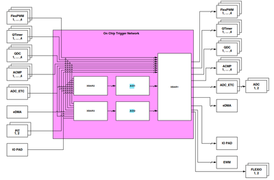
Analyzing the reference manual in the section "Chapter 81 On Chip Cross Triggers Overview," I came across the following diagram:

Upon analyzing the diagram, it appears that the following flow is possible:
IO PAD --> XBAR2/XBAR3 --> AOI --> XBAR1 --> FlexPWM
To my surprise, when examining the section "4.6 XBAR Resource Assignments," IO PAD is not listed as a possible input for XBAR2 and XBAR3. However, it is available for XBAR1. Unfortunately, XBAR1 does not allow me to perform the AND operation on the signals.
Therefore, I have the following questions:
Why does the diagram show IO PAD as an input for XBAR2 and XBAR3, but it is not listed in the resource assignments?
Is it possible to achieve what I need? If so, how can it be done?
If it is not possible, is the diagram incorrect?
Thank you for your help.
已解决! 转到解答。
Sorry for the inconvenience, I thought you were checking this issue with your distributor, who referenced this community post.
The IO PADs are not routed to XBAR2 and XBAR3. There appears to be an error in Figure 81-1. On-Chip Cross Trigger Network.
The best reference I can give you is the SDK example evkmimxrt1064_pwm_fault, which sets the PWM Fault inputs to CMP0 output pin through XBAR1.
You could try the signal routing you mentioned but instead of using IO PADs, use ACMPs.
Hope it helps you.
Have a nice day!
Thank you so much for your interest in our products and for using our community.
I noticed that you have another similar case, so I will follow up on this last one that I mention.
Have a nice day!
Sorry for the inconvenience, I thought you were checking this issue with your distributor, who referenced this community post.
The IO PADs are not routed to XBAR2 and XBAR3. There appears to be an error in Figure 81-1. On-Chip Cross Trigger Network.
The best reference I can give you is the SDK example evkmimxrt1064_pwm_fault, which sets the PWM Fault inputs to CMP0 output pin through XBAR1.
You could try the signal routing you mentioned but instead of using IO PADs, use ACMPs.
Hope it helps you.
Have a nice day!