
- Forums
- Product Forums
- General Purpose MicrocontrollersGeneral Purpose Microcontrollers
- i.MX Forumsi.MX Forums
- QorIQ Processing PlatformsQorIQ Processing Platforms
- Identification and SecurityIdentification and Security
- Power ManagementPower Management
- MCX Microcontrollers
- S32G
- S32K
- S32V
- MPC5xxx
- Other NXP Products
- Wireless Connectivity
- S12 / MagniV Microcontrollers
- Powertrain and Electrification Analog Drivers
- Sensors
- Vybrid Processors
- Digital Signal Controllers
- 8-bit Microcontrollers
- ColdFire/68K Microcontrollers and Processors
- PowerQUICC Processors
- OSBDM and TBDML
-
- Solution Forums
- Software Forums
- MCUXpresso Software and ToolsMCUXpresso Software and Tools
- CodeWarriorCodeWarrior
- MQX Software SolutionsMQX Software Solutions
- Model-Based Design Toolbox (MBDT)Model-Based Design Toolbox (MBDT)
- FreeMASTER
- eIQ Machine Learning Software
- Embedded Software and Tools Clinic
- S32 SDK
- S32 Design Studio
- GUI Guider
- Zephyr Project
- Voice Technology
- Application Software Packs
- Secure Provisioning SDK (SPSDK)
- Processor Expert Software
- MCUXpresso Training Hub
-
- Topics
- Mobile Robotics - Drones and RoversMobile Robotics - Drones and Rovers
- NXP Training ContentNXP Training Content
- University ProgramsUniversity Programs
- Rapid IoT
- NXP Designs
- SafeAssure-Community
- OSS Security & Maintenance
- Using Our Community
-
- Cloud Lab Forums
-
- Knowledge Bases
- ARM Microcontrollers
-
- Home
- :
- i.MX Forums
- :
- i.MX Processors
- :
- Re: iMX8M Plus Cortex-M7 JTAG Debug "Could not measure IR len. TDO is constant high"
iMX8M Plus Cortex-M7 JTAG Debug "Could not measure IR len. TDO is constant high"
- Subscribe to RSS Feed
- Mark Topic as New
- Mark Topic as Read
- Float this Topic for Current User
- Bookmark
- Subscribe
- Mute
- Printer Friendly Page
iMX8M Plus Cortex-M7 JTAG Debug "Could not measure IR len. TDO is constant high"
- Mark as New
- Bookmark
- Subscribe
- Mute
- Subscribe to RSS Feed
- Permalink
- Report Inappropriate Content
Hello,
I am currently trying to debug the Cortex-M7 coprocessor of the i.MX8MP. However, I cannot establish a connection and get the error message "Could not measure IR len. TDO is contant high".
I have already measured the physical connection several times. The pins used are: JTAG_RST, JTAG_TDO, JTAG_TCK, JTAG_TMS, JTAG_TDI, JTAG_nTRST, 3V3 and GND.
I also use the JLinkScript for the i.MX8MP (SDK_MX8MP_3RDPARTY_Patch) in combination with the J-Link Plus debug probe. What confuses me a bit is that in the JLinkScript the ResetTarget() function is empty.
The reference manual (document number: IMX8MPRM) contains the following sentence "When Arm platform access to the SDMA OnCE is enabled (that is, when the bit in the
ONCE_ENB register is set), the JTAG access is disabled." When I read the SDMAARMx_ONCE_ENB registers, there is a 0 in each register, which means that the arm platform access should be disabled, yet still I cannot connect via JTAG.
If I try to connect via SWD I just get "Cannot connect to target."
- Mark as New
- Bookmark
- Subscribe
- Mute
- Subscribe to RSS Feed
- Permalink
- Report Inappropriate Content
Hi @SegFault0,
I hope you are doing well.
"Could not measure total IR len. TDO is constant high."
From the above error, It seems that TDO pin is not properly connected or configured for JTAG.
Please refer to Table 6. JTAG recommendations and 2.2 JTAG signal termination in i.MX 8M Plus Hardware Developer’s Guide.
Thanks & Regards,
Dhruvit Vasavada
- Mark as New
- Bookmark
- Subscribe
- Mute
- Subscribe to RSS Feed
- Permalink
- Report Inappropriate Content
Hello,
I have not connected any external resistors/termination to any of the pins. The setup is Host PC <-> J-Link Plus <-> i.MX8MP JTAG port, pinout as described in my inital post.
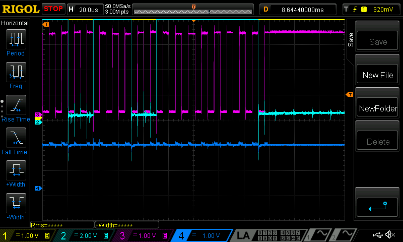
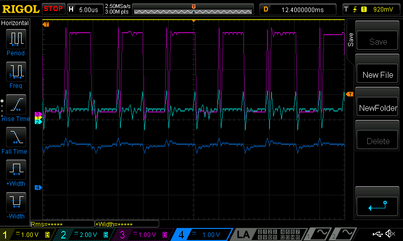 In the image above the setup was as describe (Host PC <-> J-Link Plus <-> i.MX8MP JTAG port). Channel 1 is nTRST, channel 2 is TMS, channel 3 is TCK and channel 4 is TDO. As you can see, the TCK does not look like a proper clock. In the below image, the setup was Host PC <-> J-Link Plus for the TCK pin and Host PC <-> J-Link Plus <-> i.MX8MP JTAG port for the other pins. The clock is looking much more stable compared to the image above, indicating that the clock signal is getting affected by something. I measured the resistance of the TCK pin to all other pins and found a minimum ohm value of 200k, which is still too high to affect the TCK signal.
- Mark as New
- Bookmark
- Subscribe
- Mute
- Subscribe to RSS Feed
- Permalink
- Report Inappropriate Content
Hi @SegFault0,
I hope you are doing well.
Could you please provide me with schematic for JTAG connection.
Thanks & Regards,
Dhruvit Vasavada
- Mark as New
- Bookmark
- Subscribe
- Mute
- Subscribe to RSS Feed
- Permalink
- Report Inappropriate Content
Hello,
I send you a private message regarding the schematic.
- Mark as New
- Bookmark
- Subscribe
- Mute
- Subscribe to RSS Feed
- Permalink
- Report Inappropriate Content
Hi @SegFault0,
I hope you are doing well.
Is the JTAG_MOD pin pulled down by a 10K ohm resistor?
Thanks & Regards,
Dhruvit Vasavada
- Mark as New
- Bookmark
- Subscribe
- Mute
- Subscribe to RSS Feed
- Permalink
- Report Inappropriate Content
Which pin are you referencing when you talk about the JTAG_MOD pin? The pin is not listed in the schematic I sent you neither is it listed in any other schematic.
- Mark as New
- Bookmark
- Subscribe
- Mute
- Subscribe to RSS Feed
- Permalink
- Report Inappropriate Content
Hi @SegFault0,
I hope you are doing well.
Please refer to 8.1.1.1 Muxing Options in i.MX 8M Plus Applications Processor Reference Manual for JTAG_MOD pad.

One can refer to i.MX8MP EVK reference design schematic for more information.
i.MX 8M Plus LPDDR4 EVK Compute Module Design Files (sheet 8 of SPF-46368_A3.pdf)

Thanks & Regards,
Dhruvit Vasavada
- Mark as New
- Bookmark
- Subscribe
- Mute
- Subscribe to RSS Feed
- Permalink
- Report Inappropriate Content
I have a similar problem with the i.MX8MP. It looks like the debug mode cannot be reached.
At least the RTDOBS field of the SDMAARMx_CONFIG register stays at 0 (RTD pins disabled). In the same register there is also a CSM (Context Switch Mode), which is set to 3 (dynamic) by default. Does this have to be switched to 0 (static) for debugging?
In addition in the reference manual still under 7.2.3.6.1.3.3 DEBUG mode that two things must be considered.
1 Ensure the SDMA clocks are running from the CCM.
How can I check this?
2. set the clk_gating_off pin high or use the SDMA to set ONCE_ENB[0].
Where can I find the clk_gating_off pin? This may be irrelevant, since ONCE_ENB is already set to zero.
I hope someone here can help.
- Mark as New
- Bookmark
- Subscribe
- Mute
- Subscribe to RSS Feed
- Permalink
- Report Inappropriate Content
Hi Philip
If this is your custom board please also verify the signal level on your JTAG_MOD pin.
Hope this helps.
Regards
Sinan Akman