- Forums
- Product Forums
- General Purpose MicrocontrollersGeneral Purpose Microcontrollers
- i.MX Forumsi.MX Forums
- QorIQ Processing PlatformsQorIQ Processing Platforms
- Identification and SecurityIdentification and Security
- Power ManagementPower Management
- MCX Microcontrollers
- S32G
- S32K
- S32V
- MPC5xxx
- Other NXP Products
- Wireless Connectivity
- S12 / MagniV Microcontrollers
- Powertrain and Electrification Analog Drivers
- Sensors
- Vybrid Processors
- Digital Signal Controllers
- 8-bit Microcontrollers
- ColdFire/68K Microcontrollers and Processors
- PowerQUICC Processors
- OSBDM and TBDML
-
- Solution Forums
- Software Forums
- MCUXpresso Software and ToolsMCUXpresso Software and Tools
- CodeWarriorCodeWarrior
- MQX Software SolutionsMQX Software Solutions
- Model-Based Design Toolbox (MBDT)Model-Based Design Toolbox (MBDT)
- FreeMASTER
- eIQ Machine Learning Software
- Embedded Software and Tools Clinic
- S32 SDK
- S32 Design Studio
- GUI Guider
- Zephyr Project
- Voice Technology
- Application Software Packs
- Secure Provisioning SDK (SPSDK)
- Processor Expert Software
- MCUXpresso Training Hub
-
- Topics
- Mobile Robotics - Drones and RoversMobile Robotics - Drones and Rovers
- NXP Training ContentNXP Training Content
- University ProgramsUniversity Programs
- Rapid IoT
- NXP Designs
- SafeAssure-Community
- OSS Security & Maintenance
- Using Our Community
-
- Cloud Lab Forums
-
- Knowledge Bases
- ARM Microcontrollers
- i.MX Processors
- Identification and Security
- Model-Based Design Toolbox (MBDT)
- QorIQ Processing Platforms
- S32 Automotive Processing Platform
- Wireless Connectivity
- CodeWarrior
- MCUXpresso Suite of Software and Tools
- MQX Software Solutions
-
Hello,
I have schematic references for most of LPDDR3 and this MCU but RAM module that I want to use is 8Gb from Micron. And this particular module miss some pins. Its 1 x 8Gb Die module 32bit, ball/pad description attached. As you can see command and address inputs are together. Which means that RAS#, CAS#, WE# pins aren't present and also bank address input pins.
My question is do I connect these CA[9:0] pins on regular address pins on MCU and what to do with rest unused pins on it? (command pins on MCU)
已解决! 转到解答。
Hello Indir Okanovic,
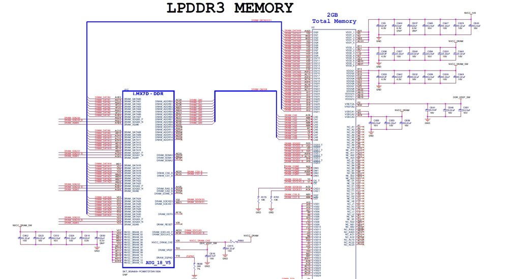
LPDDR3 does uses different connections than regular DDR3. You may find an example on how to connect these on the following diagram.

I hope this helps!
Regards,
Hi,
I have two questions regarding this sheet:
- As I want to use RAM memory normally. is the lower part of scheme that is attached necessary? Meaning can I just use regular NVCC_DRAM and DDR_VREF ( not *_SW outputs ) for corresponding power rails on MCU and LPDDR3?
- I noticed that 8 bit lanes on DDR side are scrambled, and also their group order (3rd 8bit lane, than 1st...). So I can set them up for easier layout as long as I am in group. 0-7, 8-15.... ; and I follow the group order also for DQS, DM?
Tnx,
Regards
EDIT: file attached
For anybody that is looking for an answer to same question that I had, I got it via support tickets. (tnx to Igor)
- As I have DDR_VREF directly from PMIC voltage divider isnt needed in my case.
- DDR 8bit data group can be shuffled for easier layout
hi!
I'm where you was before, just to clarify:
where the NVCC_DRAM_SW is connected Is the same connection than NVCC_DRAM? (1.35V, I'm using the PF3000 as a power manager, it it's relevant)
The shuffling of the data lines helps the layout of the PCB, but they are not banks? I mean D[16..23] is connected to D[0..7] and SDQ2 to SDQ0, this is clear, but in the next bank D5 is connected to D8, D0 to D9, D3 to D10 and so on, is this correct? (I guess the memory is stored and recovered in the same way and the memory chip don't really cares, but I don't understand yet the meaning of the function of the SDQ/DQM lines)
BTW the complete schematic who contains the drawing above is available somewhere?