- Forums
- Product Forums
- General Purpose MicrocontrollersGeneral Purpose Microcontrollers
- i.MX Forumsi.MX Forums
- QorIQ Processing PlatformsQorIQ Processing Platforms
- Identification and SecurityIdentification and Security
- Power ManagementPower Management
- MCX Microcontrollers
- S32G
- S32K
- S32V
- MPC5xxx
- Other NXP Products
- Wireless Connectivity
- S12 / MagniV Microcontrollers
- Powertrain and Electrification Analog Drivers
- Sensors
- Vybrid Processors
- Digital Signal Controllers
- 8-bit Microcontrollers
- ColdFire/68K Microcontrollers and Processors
- PowerQUICC Processors
- OSBDM and TBDML
-
- Solution Forums
- Software Forums
- MCUXpresso Software and ToolsMCUXpresso Software and Tools
- CodeWarriorCodeWarrior
- MQX Software SolutionsMQX Software Solutions
- Model-Based Design Toolbox (MBDT)Model-Based Design Toolbox (MBDT)
- FreeMASTER
- eIQ Machine Learning Software
- Embedded Software and Tools Clinic
- S32 SDK
- S32 Design Studio
- GUI Guider
- Zephyr Project
- Voice Technology
- Application Software Packs
- Secure Provisioning SDK (SPSDK)
- Processor Expert Software
- MCUXpresso Training Hub
-
- Topics
- Mobile Robotics - Drones and RoversMobile Robotics - Drones and Rovers
- NXP Training ContentNXP Training Content
- University ProgramsUniversity Programs
- Rapid IoT
- NXP Designs
- SafeAssure-Community
- OSS Security & Maintenance
- Using Our Community
-
- Cloud Lab Forums
-
- Knowledge Bases
- ARM Microcontrollers
-
why SRAM segmented to two banks?
09-16-2020
12:43 AM
1,231 次查看
Ahmad_bozorgi
Contributor II
hello, I select S32K14x as MCU for my project. when I read datasheet and user manual, noticed that there is two bank (32KB as SRAM_L and 28KB as SRAM_U) in chip. they are separated from each other in bus access way. 1. my question is about advantages of this method in MCU? (why there is two SRAM block?) 2. accessing time is different for them? 3. when we should use each of two banks? Thanks.
3 回复数
09-18-2020
09:59 PM
1,210 次查看
Ahmad_bozorgi
Contributor II
Thanks for reply.
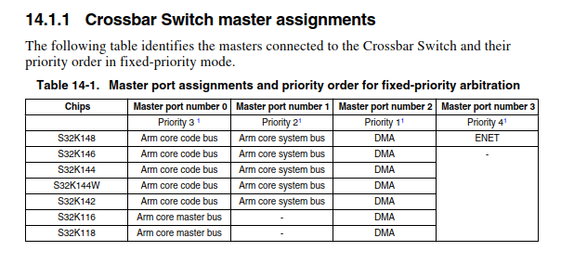
what is the mean of Core System Bus? which part of MCU is in this section?
can use both Core Code and Core System bus simultaneously? (what is application in this mode?)
09-17-2020
03:54 AM
1,215 次查看
NXP TechSupport
It offers certain advantage for performance optimization.
SRAM_L offers single-cycle access for core code bus whilst SRAM_U offers single-cycle access for core system bus. Other accesses are backdoor and these take two clocks.
