- Forums
- Product Forums
- General Purpose MicrocontrollersGeneral Purpose Microcontrollers
- i.MX Forumsi.MX Forums
- QorIQ Processing PlatformsQorIQ Processing Platforms
- Identification and SecurityIdentification and Security
- Power ManagementPower Management
- MCX Microcontrollers
- S32G
- S32K
- S32V
- MPC5xxx
- Other NXP Products
- Wireless Connectivity
- S12 / MagniV Microcontrollers
- Powertrain and Electrification Analog Drivers
- Sensors
- Vybrid Processors
- Digital Signal Controllers
- 8-bit Microcontrollers
- ColdFire/68K Microcontrollers and Processors
- PowerQUICC Processors
- OSBDM and TBDML
-
- Solution Forums
- Software Forums
- MCUXpresso Software and ToolsMCUXpresso Software and Tools
- CodeWarriorCodeWarrior
- MQX Software SolutionsMQX Software Solutions
- Model-Based Design Toolbox (MBDT)Model-Based Design Toolbox (MBDT)
- FreeMASTER
- eIQ Machine Learning Software
- Embedded Software and Tools Clinic
- S32 SDK
- S32 Design Studio
- GUI Guider
- Zephyr Project
- Voice Technology
- Application Software Packs
- Secure Provisioning SDK (SPSDK)
- Processor Expert Software
- MCUXpresso Training Hub
-
- Topics
- Mobile Robotics - Drones and RoversMobile Robotics - Drones and Rovers
- NXP Training ContentNXP Training Content
- University ProgramsUniversity Programs
- Rapid IoT
- NXP Designs
- SafeAssure-Community
- OSS Security & Maintenance
- Using Our Community
-
- Cloud Lab Forums
-
- Knowledge Bases
- ARM Microcontrollers
- i.MX Processors
- Identification and Security
- Model-Based Design Toolbox (MBDT)
- QorIQ Processing Platforms
- S32 Automotive Processing Platform
- Wireless Connectivity
- CodeWarrior
- MCUXpresso Suite of Software and Tools
- MQX Software Solutions
-
FTM2 Output Modulation
Hello all,
I'd gone through the thread FTM2 for Modulation & would like to understand more about the implementation of the same.
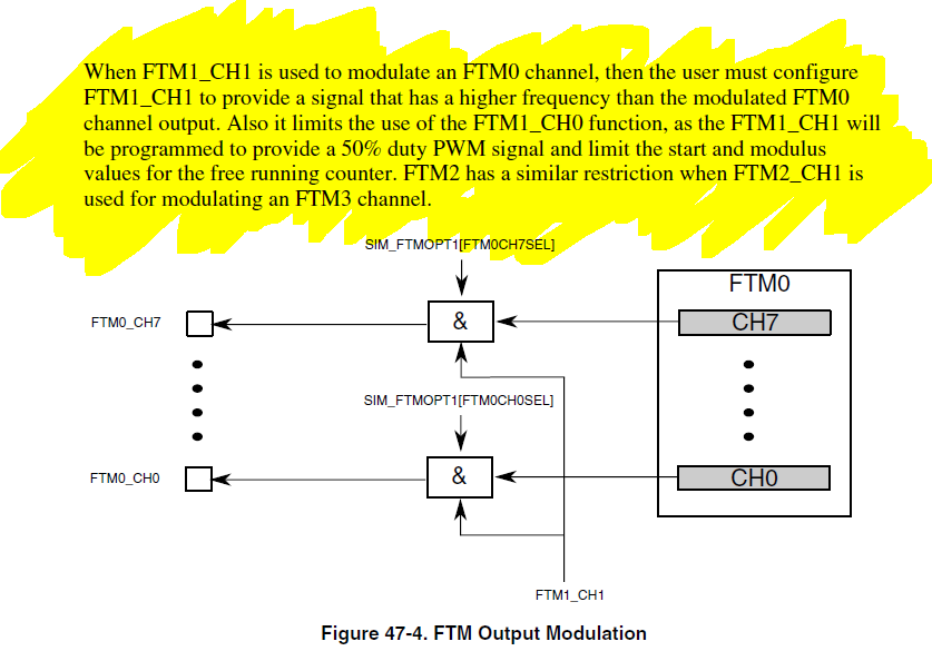
Can anyone help what exactly it mean using OUTSEL bits in SIM->FTMOPT1 help for FTM0 & FTM3 Modulation?
Does it mean it will help in the channel match with CH1?
if I keep SIM->FTMOPT1=SIM_FTMOPT1_FTM3_OUTSEL(0x01);
FTM2CH1 will give a modulated signal instead of channel FTM3CH0?
Clarify me in this regard.
Raju.
Hello all,
I got a question again.
Can anyone explain what actual the below lines explain?
Thanks in advance,
Raju
Hi Raju,
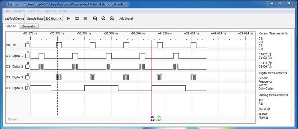
It is difficult to describe in text, you can refer to the pictures in Modulated PWM waveform Generation
The Original waveform of FTM0_CH0~FTM0_CH7 should be like D0 D1.
The modulated waveform of FTM0_CH0~FTM0_CH7 will be like D2 D3.
The high frequency 50% duty PWM is FTM1_CH1.
Best Regards,
Robin
-----------------------------------------------------------------------------------------------------------------------
Note: If this post answers your question, please click the Correct Answer button. Thank you!
-----------------------------------------------------------------------------------------------------------------------
Hi Robin,
Thanks again for your swift response.
I have few questions.
1. Is FTM2 generating a 50% duty modulated signal?
2. In the case of modulated frequency i.e, D2 & D3, how actually channel duty cycle is varied?
3. Is there anything we need to do via hardware so as use FTM2 for modulating frequency?
4. Can you share an application note or code for describing such a scenario?
Thanks in advance,
Raju
Let me try to add comment to your questions.
1. It generates a 50% duty cycle pwm output. The FAULT input signal performs the modulation.
2. Same as usual for PWM functions. MOD register is the period and CnV register is the duty.
3. Yes, you must hard wire the FTM0 outputs (ch0 and ch2) to the FTM1 and FTM2 FAULT input pins
4. Code was shared on the post which Robin referred: https://community.nxp.com/thread/450366
hope this helps.

