LS1046ARDB Clock Circuit

キャンセル
次の結果を表示 
表示  限定  | 次の代わりに検索 
もしかして: 

LS1046ARDB Clock Circuit

ソリューションへジャンプ
949件の閲覧回数
matthej
Contributor II
 

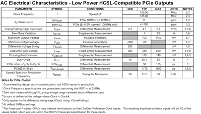
The LS1046ARDB  eval board uses a 6V49205 clock generator which produces a HCSL output, but the LS1046 input is LVDS. I have attached the section of the 6V49205 datasheet which describes the output clock:
 
matthej_2-1622645344468.png


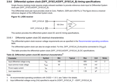
The clock input is specified in this attached picture.
 
matthej_3-1622645455719.png


The eval board uses 50 ohm to ground termination on the output. I am having a hard time in seeing how this interface will work.

If you look at note 7 for the clock output it says the amplitude will be 1/2 of what is listed but the swing looks to be greater than the input can handle.

Output swing (max): 1150/2 - (-300/2) = 725mV, but the input says it can only handle a 600mV

Am I missing something here?

Thanks!

0 件の賞賛
返信
1 解決策
934件の閲覧回数
ufedor
NXP Employee
NXP Employee

You also have to consider divider consisting of serial and ground resistors:

serial.jpgground.jpg

元の投稿で解決策を見る

3 返答(返信)
944件の閲覧回数
ufedor
NXP Employee
NXP Employee

Which exactly LS1046A clock is in question?

0 件の賞賛
返信
941件の閲覧回数
matthej
Contributor II

The DIFF_SYSCLK and DIFF_SYSCLK_B clock inputs

0 件の賞賛
返信
935件の閲覧回数
ufedor
NXP Employee
NXP Employee

You also have to consider divider consisting of serial and ground resistors:

serial.jpgground.jpg