- Forums
- Product Forums
- General Purpose MicrocontrollersGeneral Purpose Microcontrollers
- i.MX Forumsi.MX Forums
- QorIQ Processing PlatformsQorIQ Processing Platforms
- Identification and SecurityIdentification and Security
- Power ManagementPower Management
- MCX Microcontrollers
- S32G
- S32K
- S32V
- MPC5xxx
- Other NXP Products
- Wireless Connectivity
- S12 / MagniV Microcontrollers
- Powertrain and Electrification Analog Drivers
- Sensors
- Vybrid Processors
- Digital Signal Controllers
- 8-bit Microcontrollers
- ColdFire/68K Microcontrollers and Processors
- PowerQUICC Processors
- OSBDM and TBDML
- S32M
-
- Solution Forums
- Software Forums
- MCUXpresso Software and ToolsMCUXpresso Software and Tools
- CodeWarriorCodeWarrior
- MQX Software SolutionsMQX Software Solutions
- Model-Based Design Toolbox (MBDT)Model-Based Design Toolbox (MBDT)
- FreeMASTER
- eIQ Machine Learning Software
- Embedded Software and Tools Clinic
- S32 SDK
- S32 Design Studio
- GUI Guider
- Zephyr Project
- Voice Technology
- Application Software Packs
- Secure Provisioning SDK (SPSDK)
- Processor Expert Software
- MCUXpresso Training Hub
-
- Topics
- Mobile Robotics - Drones and RoversMobile Robotics - Drones and Rovers
- NXP Training ContentNXP Training Content
- University ProgramsUniversity Programs
- Rapid IoT
- NXP Designs
- SafeAssure-Community
- OSS Security & Maintenance
- Using Our Community
-
- Cloud Lab Forums
-
- Knowledge Bases
- ARM Microcontrollers
- i.MX Processors
- Identification and Security
- Model-Based Design Toolbox (MBDT)
- QorIQ Processing Platforms
- S32 Automotive Processing Platform
- Wireless Connectivity
- CodeWarrior
- MCUXpresso Suite of Software and Tools
- MQX Software Solutions
-
- Home
- :
- 软件论坛
- :
- Processor Expert软件
- :
- Re: Processor Expert for Vybrid: General Questions
Processor Expert for Vybrid: General Questions
Processor Expert for Vybrid: General Questions
We had a meeting with a customer today. While we were able to answer technical questions about Vybrid and what the calibration tests are doing and what they mean, there were a number of questions about the Processor
Expert software that we need help with:
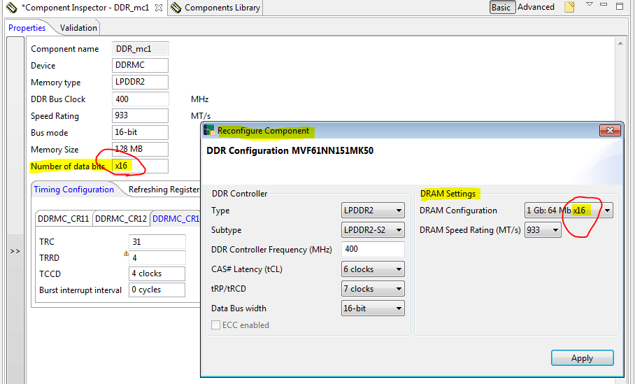
1) On the summary page, there are basic selection boxes for memory type, Speed Rating, etc. There is a box for Bus Mode which should be set to 16-bit when all 16 data bits of Vybrid are being used. What is the purpose of the box
for "Number of Data Bits"? Does this refer to the data width of the attached DDR device? What effect does this box have on the Register Settings?
2) In conjunctions with #1, when the "Number of Data Bits" box is changed from x8 to x16, Processor Expert shows more register errors (boxes change to red with a note that values do not meet JEDEC requirements). This also happens when the value of the “Speed Rating” box is changed. Do you know why all these error messages are popping up? When the JEDEC standards are consulted, the values seem to be correct. Is there a file that holds these error equations, or are they compiled in the Processor Expert code?
3) Is there an easy way to export the MMDC (CR/PHY) values to a file that can be used to create the u-boot file for the MMDC? Or do these values need to be copied by hand?
Thank you very much for your assistance,
Mark
Hi Mark,
I'm sorry it took me longer time to investigate all details because I didn't seen Vybrid and Driver Suite for more than year and half, but I have found following:
1) Property "Number of data bits" is defined by the external DRAM module configuration (see the selected value also within a "Reconfigure..." dialog under DRAM Settings) and it is intended mostly for the tool internal calculations of DDR timing parameters. When it changes it means like the DRAM module configuration has changed and re-calculation of timing parameters is performed which may lead to some register modifications.
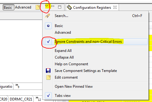
2) In general, DDR dynamic timing parameters are all calculated using equations defined within Init_DDR_VYBRID component internal scripts (CHG) which is not originally intended for end user modifications. In fact it's encoded and included in the common PEx components files package inside the "ProcessorExpert\" structure. However, the errors reported by the component complaining about JEDEC can be easily overcome in "Ignore Constraints and non-Critical Errors" mode of Component inspector for the actual active component. When enabled, all reported component errors will change to "Ignored error: ..." and the code generation or DDR validation tests can be started as without those errors. Please note that this mode is intended for advanced users, because the tool accepts potentially wrong configuration (even false positive) and it's up to the user's responsibility what actions he takes with such configuration.
3) Unfortunately, there's no direct way in Driver Suite v10.4.x how to export any peripheral register values easily from the tool UI. However, DDR Validation tool creates some log during the processing (e.g. when operational test is performed regardless of the result), so the tool generates some temporary script and log files which can be found in host OS file system under the Driver Suite eclipse workspace respective project folder location. Name of such temporary folder starts with ".Init_DDR_VYBRID_" following the current device variant. There're log and scripts sub-folders inside that temporary folder and if you go to the "log" you can see some file like "test_operational_tests_0_0_.log" (see attached example) which have logged all writes to the device registers as they're applied to run the operational test on device. You can simply get the real values for DDRMC modified registers according to address out of this log. Maybe one more comment yet, only the writable and really modified registers are mentioned in this log file. It does mean that the unmodified registers (the ones that have the same init.value as the after reset displayed in the Registers view UI) are not listed here. Anyway, content of that log file still need further processing on the end user side in order to get the register values in a form suitable for u-boot processing.
Hope this helps.
Regards,
Petr Z.

