
- Forums
- Product Forums
- General Purpose MicrocontrollersGeneral Purpose Microcontrollers
- i.MX Forumsi.MX Forums
- QorIQ Processing PlatformsQorIQ Processing Platforms
- Identification and SecurityIdentification and Security
- Power ManagementPower Management
- Wireless ConnectivityWireless Connectivity
- RFID / NFCRFID / NFC
- Advanced AnalogAdvanced Analog
- Neural Processing UnitsNeural Processing Units
- MCX Microcontrollers
- S32G
- S32K
- S32V
- MPC5xxx
- Other NXP Products
- S12 / MagniV Microcontrollers
- Powertrain and Electrification Analog Drivers
- Sensors
- Vybrid Processors
- Digital Signal Controllers
- 8-bit Microcontrollers
- ColdFire/68K Microcontrollers and Processors
- PowerQUICC Processors
- OSBDM and TBDML
- S32M
- S32Z/E
-
- Solution Forums
- Software Forums
- MCUXpresso Software and ToolsMCUXpresso Software and Tools
- CodeWarriorCodeWarrior
- MQX Software SolutionsMQX Software Solutions
- Model-Based Design Toolbox (MBDT)Model-Based Design Toolbox (MBDT)
- FreeMASTER
- eIQ Machine Learning Software
- Embedded Software and Tools Clinic
- S32 SDK
- S32 Design Studio
- GUI Guider
- Zephyr Project
- Voice Technology
- Application Software Packs
- Secure Provisioning SDK (SPSDK)
- Processor Expert Software
- Generative AI & LLMs
-
- Topics
- Mobile Robotics - Drones and RoversMobile Robotics - Drones and Rovers
- NXP Training ContentNXP Training Content
- University ProgramsUniversity Programs
- Rapid IoT
- NXP Designs
- SafeAssure-Community
- OSS Security & Maintenance
- Using Our Community
-
- Cloud Lab Forums
-
- Knowledge Bases
- ARM Microcontrollers
- i.MX Processors
- Identification and Security
- Model-Based Design Toolbox (MBDT)
- QorIQ Processing Platforms
- S32 Automotive Processing Platform
- Wireless Connectivity
- CodeWarrior
- MCUXpresso Suite of Software and Tools
- MQX Software Solutions
- RFID / NFC
- Advanced Analog
- Neural Processing Units
-
- NXP Tech Blogs
- Home
- :
- 製品フォーラム
- :
- PowerQUICCプロセッサ
- :
- T1022 interface with DDR4 SDRAM
T1022 interface with DDR4 SDRAM
- RSS フィードを購読する
- トピックを新着としてマーク
- トピックを既読としてマーク
- このトピックを現在のユーザーにフロートします
- ブックマーク
- 購読
- ミュート
- 印刷用ページ
- 新着としてマーク
- ブックマーク
- 購読
- ミュート
- RSS フィードを購読する
- ハイライト
- 印刷
- 不適切なコンテンツを報告
Hello All,
We have a custom board where we have connected the DDR4 interface of T1022 processor to 5 nos. of DDR4 SDRAM ICs ( 64-bit data-bus + 8-bit ECC). The part number of the SDRAM is MT40A512M16TB-062E. We are not using any SPD EEPROM in the design, instead we are hard-coding the SPD bytes.
We are not able to boot the processor with the said SPD bytes. Some locations are read-writeable in the DDR4 address, some are not. We have some queries to help with the debugging:
1) Should we configure the SPD bytes as per the DDR4 capability (3200 MT/s) or as per the processor capability (1600 MT/s)?
2) Bytes 41-45 do not exist in the kernel we are currently using but as per the SPD description of the said bytes, we think this is an important field (TWRmin, TWTR_Lmin, TWTR_Smin). Please suggest.
3) We had referenced the FRWY-LS1046A Evaluation board for the schematic connections. (#https://www.nxp.com/design/software/qoriq-developer-resources/ls1046a-freeway-board:FRWY-LS1046A) Is it possible that we can get the SPD bytes that have been programmed on that board?
Any help regarding this is highly appreciated.
Thanks and Regards,
Souvik
解決済! 解決策の投稿を見る。
- 新着としてマーク
- ブックマーク
- 購読
- ミュート
- RSS フィードを購読する
- ハイライト
- 印刷
- 不適切なコンテンツを報告
Please change the following ddr register values (for registers not listed please use default reset values for example for DQ_MAP =0x0):
Offset Register Name Generated
0x000 CS0_BNDS 000000FF
0x080 CS0_CONFIG 80010412
0x100 TIMING_CFG_3 01111000
0x104 TIMING_CFG_0 d1550018
0x108 TIMING_CFG_1 CAC60C52
0x10C TIMING_CFG_2 0048C11C
0x110 DDR_SDRAM_CFG E5040000
0x114 DDR_SDRAM_CFG_2 00401010
0x118 DDR_SDRAM_MODE 01010214
0x124 DDR_SDRAM_INTERVAL 18600618
0x130 DDR_SDRAM_CLK_CNTL 02000000
0x160 TIMING_CFG_4 00000002
0x164 TIMING_CFG_5 04401400
0x16C TIMING_CFG_7 23300000
0x170 DDR_ZQ_CNTL 8A090705
0x174 DDR_WRLVL_CNTL 86550606
0x190 DDR_WRLVL_CNTL_2 06060606
0x194 DDR_WRLVL_CNTL_3 06060606
0x220 DDR_SDRAM_MODE_9 00000500
0x224 DDR_SDRAM_MODE_10 04400000
0x250 TIMING_CFG_8 03116600
0xB28 DDRCDR_1 80040000
0xB2C DDRCDR_2 0000A1C1
if there is failures with above settings. please send a fresh register dump via ccs after failure. also make sure the DRAM reset signal matches the HRESET signal assertion, deassertion timing.
- 新着としてマーク
- ブックマーク
- 購読
- ミュート
- RSS フィードを購読する
- ハイライト
- 印刷
- 不適切なコンテンツを報告
@yipingwang , thank you for your reply.
Sorry if I said it wrong but by hard-coding the SPD I meant to say that we had fixed the register settings as you have done in the shared example.
@prakashram72 thank you for your reply too. We have programmed the SPD parameters as per the DDR4 datasheet pertaining to speed of 1600MT/s.
We are still not able to access the DDR4 registers. When we use the TRACE32 software to write on the DDR4 addresses, some locations can be written while some could not be written.
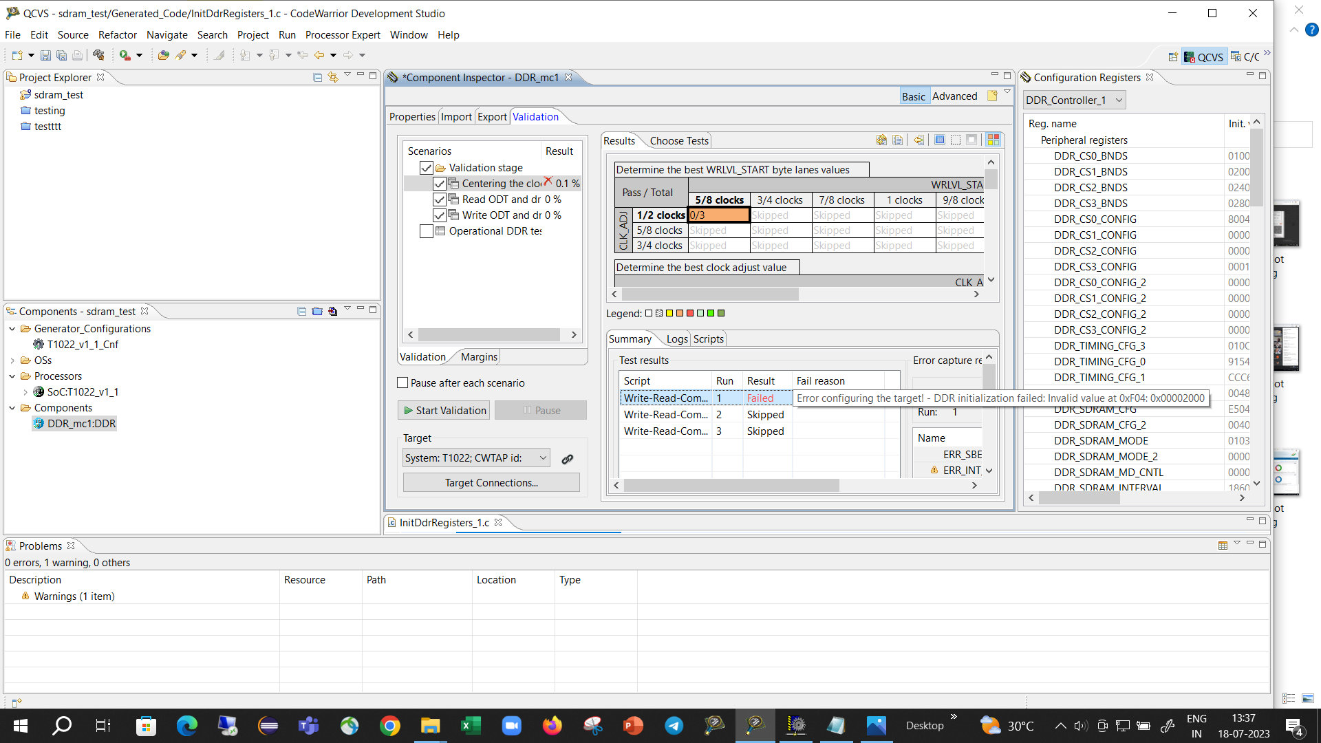
We are also using the QCVS tool for DDR validation using CodeWarrior TAP tool. The error message comes as "DDR Initialization failed. D_INIT was not cleared by hardware" and "ERR_DETECT register has non-zero value". And in some cases we get the error message as "Error configuring the Target!-DDR Initialization failed: Invalid value at 0xF04:0x00002000". (Attached error.png for your reference).
In case of ERR_DETECT register, as we can read from the TRACE32 device, the bits about MME, SSBE, ACE, CDE, SBE shows ERROR.
I am also attaching the DDR controller schematic for your reference.
Thanks and Regards,
Souvik
- 新着としてマーク
- ブックマーク
- 購読
- ミュート
- RSS フィードを購読する
- ハイライト
- 印刷
- 不適切なコンテンツを報告
If there is no DDR SPD on your custom board, please create a QCVS DDR project with default configuration, then modify Properties panel according to your DDR datasheet.
Please refer to section "1.1.1.2 Configure DDR controller" in the attached QCVS DDR user manual.
We will review your DDR schematic.
- 新着としてマーク
- ブックマーク
- 購読
- ミュート
- RSS フィードを購読する
- ハイライト
- 印刷
- 不適切なコンテンツを報告
- 新着としてマーク
- ブックマーク
- 購読
- ミュート
- RSS フィードを購読する
- ハイライト
- 印刷
- 不適切なコンテンツを報告
please provide the ddr register dump via ccs after failure:
How to get register dump via ccs
This is for debug use only.
1) Open a CCS window (C:\Freescale\CW4NET_vxxxx\Common\CCS\bin\ccs.exe)
2) Physical connection: USB to PC, JTAG to the customer board.
3) SW connection: in the ccs window type:
delete all
config cc cwtap
ccs::config_chain t1040
display ccs::read_mem 0 0x30000 0x8000 4 2 1024
ccs::write_mem 0 0x30000 0x8FB0 4 2 0x10000000
display ccs::read_mem 0 0x30000 0x8000 4 2 1024
- 新着としてマーク
- ブックマーク
- 購読
- ミュート
- RSS フィードを購読する
- ハイライト
- 印刷
- 不適切なコンテンツを報告
Hello,
Please find the dump of the ccs console inputs attached to this reply.
In place of t1040, we had written t1020 as we are using the t1022 processor and the scanboard command returns t1020/t1021 as the detected device.
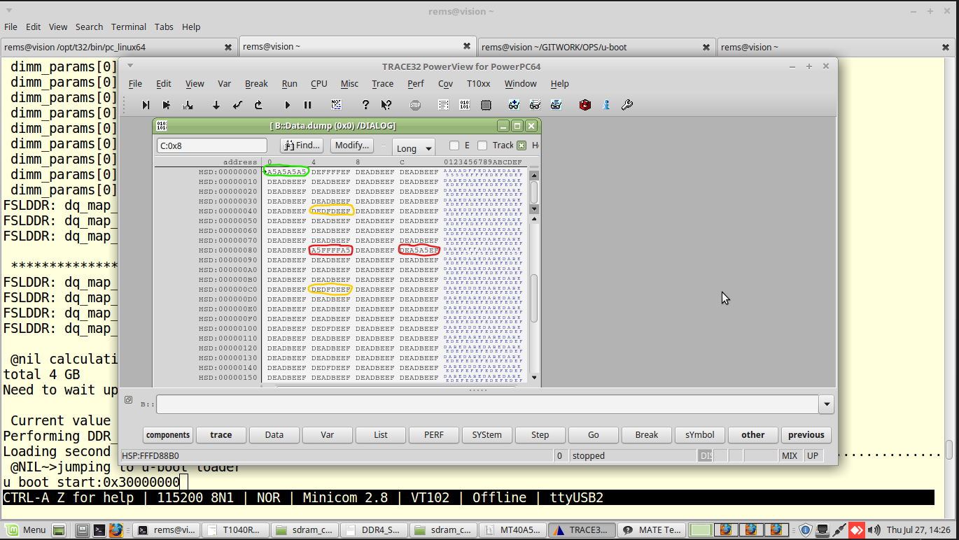
There are two observations during use of Trace32 tool that I would like to share.
1) After disabling ECC, we are only left with ACE (automatic calibration) error in the ERR_DETECT register, as can be read using the Trace32 Tool. We are able to read and write in memory locations using the trace32 tool with lesser errors. Attached is the screenshot with the values, as you can see the field marked in GREEN was DEADBEEF earlier, we could write A5A5A5A5 onto that location successfully without errors. However, when we write in the location as shown in RED the same value (i.e. A5A5A5A5) we find that the values change to as shown. The value at the location changes to A5FFFFA5 and the value in the adjacent memory location (also shown by RED) changes from DEADBEEF to DEA5A5EF. The above thing happens in the locations shown by YELLOW marks. Like we can observe a pattern in the occurrences.
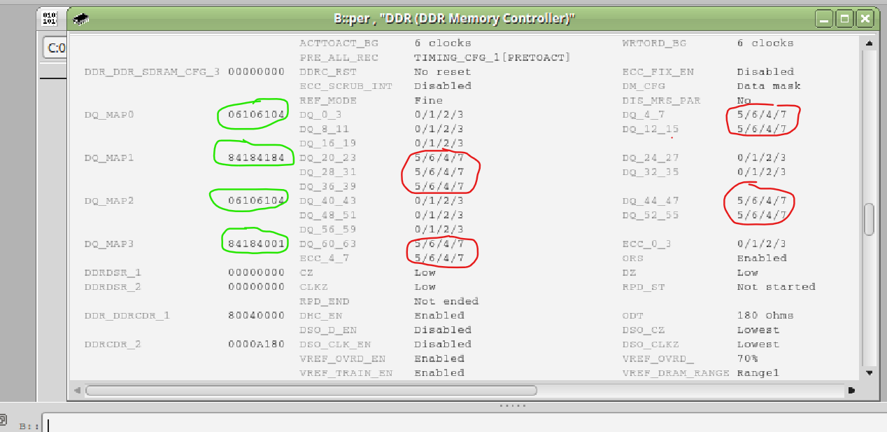
2) Also, in the DQ mapping bits, if we look in the values shown by the register values, we get the correct mapping that is present in the schematic connections (shown by GREEN). However, the trace32 values that are incorrect as per my understanding (shown by RED). It would be great if could confirm the DQ mapping values from the schematic shared in the previous reply.
Please note that all of these are happening when the ECC is disabled.
- 新着としてマーク
- ブックマーク
- 購読
- ミュート
- RSS フィードを購読する
- ハイライト
- 印刷
- 不適切なコンテンツを報告
Please change the following ddr register values (for registers not listed please use default reset values for example for DQ_MAP =0x0):
Offset Register Name Generated
0x000 CS0_BNDS 000000FF
0x080 CS0_CONFIG 80010412
0x100 TIMING_CFG_3 01111000
0x104 TIMING_CFG_0 d1550018
0x108 TIMING_CFG_1 CAC60C52
0x10C TIMING_CFG_2 0048C11C
0x110 DDR_SDRAM_CFG E5040000
0x114 DDR_SDRAM_CFG_2 00401010
0x118 DDR_SDRAM_MODE 01010214
0x124 DDR_SDRAM_INTERVAL 18600618
0x130 DDR_SDRAM_CLK_CNTL 02000000
0x160 TIMING_CFG_4 00000002
0x164 TIMING_CFG_5 04401400
0x16C TIMING_CFG_7 23300000
0x170 DDR_ZQ_CNTL 8A090705
0x174 DDR_WRLVL_CNTL 86550606
0x190 DDR_WRLVL_CNTL_2 06060606
0x194 DDR_WRLVL_CNTL_3 06060606
0x220 DDR_SDRAM_MODE_9 00000500
0x224 DDR_SDRAM_MODE_10 04400000
0x250 TIMING_CFG_8 03116600
0xB28 DDRCDR_1 80040000
0xB2C DDRCDR_2 0000A1C1
if there is failures with above settings. please send a fresh register dump via ccs after failure. also make sure the DRAM reset signal matches the HRESET signal assertion, deassertion timing.
- 新着としてマーク
- ブックマーク
- 購読
- ミュート
- RSS フィードを購読する
- ハイライト
- 印刷
- 不適切なコンテンツを報告
Hello,
Sorry for the late reply and I come with a good news, that the SDRAMs have been initialized successfully. We used the register values that were shared by you. Instead of using default values of DQ mapping, we used the values as per our design. Attaching the .regs file exported from the tool.
We are grateful for your help in this. Thanks a lot.
- 新着としてマーク
- ブックマーク
- 購読
- ミュート
- RSS フィードを購読する
- ハイライト
- 印刷
- 不適切なコンテンツを報告
1) for the SPD you should enter the values from the DDR4 datasheet.
2) if not present try it without it.
3) when discrete DRAM is soldered on the board, the DDR controller registers are programed via fixed register setting or mocked SPD is used. I have not seen any customers do the hard code the SPD (as it is read from a DIMM).
for the mocked program the ddr_raw_timing[] and enable/set the DEF (#ifdef CONFIG_SYS_DDR_RAW_TIMING)
for the fixed DDR controller register: program the fixed_ddr_pram for fixed DDR controller registers. and disable the DEF (#ifdef CONFIG_SYS_DDR_RAW_TIMING).
for example:
#ifdef CONFIG_SYS_DDR_RAW_TIMING
/* DDR model number: MT40A512M16JY-083E:B */
struct dimm_params ddr_raw_timing = {
.n_ranks = 1,
.rank_density = 4294967296u,
.capacity = 4294967296u,
.primary_sdram_width = 64,
.ec_sdram_width = 8,
.rdimm = 0,
.mirrored_dimm = 0,
.n_row_addr = 16,
.n_col_addr = 10,
.bank_group_bits = 1,
.edc_config = 2,
.burst_lengths_bitmask = 0x0c,
.tckmin_x_ps = 750,
.tckmax_ps = 1900,
.caslat_x = 0x0001FFE00,
.taa_ps = 13500,
.trcd_ps = 13500,
.trp_ps = 13500,
.tras_ps = 33000,
.trc_ps = 46500,
.twr_ps = 15000,
.trfc1_ps = 350000,
.trfc2_ps = 260000,
.trfc4_ps = 160000,
.tfaw_ps = 30000,
.trrds_ps = 5300,
.trrdl_ps = 6400,
.tccdl_ps = 5355,
.refresh_rate_ps = 7800000,
.dq_mapping[0] = 0x0,
.dq_mapping[1] = 0x0,
.dq_mapping[2] = 0x0,
.dq_mapping[3] = 0x0,
.dq_mapping[4] = 0x0,
.dq_mapping_ors = 0,
.rc = 0x1f,
};
- 新着としてマーク
- ブックマーク
- 購読
- ミュート
- RSS フィードを購読する
- ハイライト
- 印刷
- 不適切なコンテンツを報告
Hi @sarkarsouvik ,
Here are some suggestions that might help you with your problem:
1) The SPD bytes should be configured as per the processor capability. In your case, it should be 1600 MT/s. The SPD bytes are used to inform the memory controller of the module's size, data width, speed, and other parameters, so they should match the capabilities of the controller, not the memory.
2) Bytes 41-45 are indeed important as they define the minimum write recovery time (TWRmin), the minimum internal write to read command delay for different bank group (TWTR_Lmin), and the minimum internal write to read command delay for same bank group (TWTR_Smin). If these bytes are not defined in your kernel, you might need to update your kernel or manually define these parameters.
3) Unfortunately, we cannot provide the SPD bytes that have been programmed on the FRWY-LS1046A Evaluation board. However, you can refer to the LS1046A Freeway Board User Guide for more information on how the board is set up. You can also refer to the QorIQ SDK User's Guide for more information on how to configure the SPD bytes.
Also, make sure that your DDR4 SDRAM ICs are correctly connected to the T1022 processor and that the power supply and clock signals are stable. You can use the Hardware Design Checklist for the QorIQ T Series as a reference.
Regards,
Prakash